Answered step by step
Verified Expert Solution
Question
1 Approved Answer
In Web2, Figure 3.3a (page 23), assuming the counter has been misconfigured so that the input signal to FFO is, instead of HIGH as displayed,
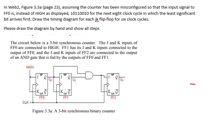
In Web2, Figure 3.3a (page 23), assuming the counter has been misconfigured so that the input signal to FFO is, instead of HIGH as displayed, 10110010 for the next eight clock cycle in which the least significant bit arrives first. Draw the timing diagram for each jk flip-flop for six clock cycles. Please draw the diagram by hand and show all steps The circuit below is a 3-bit synchronous counter. The J and K inputs of FF0 are connected to HIGH. FF1 has its J and K inputs connected to the output of FF0, and the J and K inputs of FF2 are connected to the output of an AND gate that is fed by the outputs of FF0 and FF1. Figure 3.3a: A 3-bit synchronous binary counter
Step by Step Solution
There are 3 Steps involved in it
Step: 1
Get Instant Access to Expert-Tailored Solutions
See step-by-step solutions with expert insights and AI powered tools for academic success
Step: 2
Step: 3
Ace Your Homework with AI
Get the answers you need in no time with our AI-driven, step-by-step assistance
Get Started