

Answered step by step
Verified Expert Solution
Question
1 Approved Answer
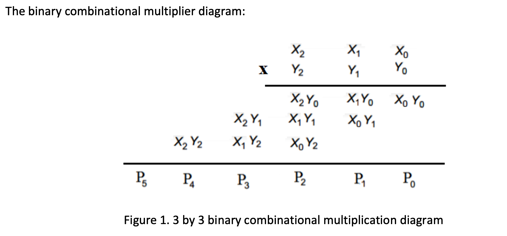
include wave simulation and test bench if possible The binary combinational multiplier diagram: X2 X Xo YO X Y2 Y X Yo Xo Yo X,
 include wave simulation and test bench if possible
Step by Step Solution
There are 3 Steps involved in it
Step: 1

Get Instant Access to Expert-Tailored Solutions
See step-by-step solutions with expert insights and AI powered tools for academic success
Step: 2

Step: 3
Ace Your Homework with AI
Get the answers you need in no time with our AI-driven, step-by-step assistance
Get Started
Principles Of Multimedia Database Systems
Authors: V.S. Subrahmanian
1st Edition
1558604669, 978-1558604667