Answered step by step
Verified Expert Solution
Question
1 Approved Answer
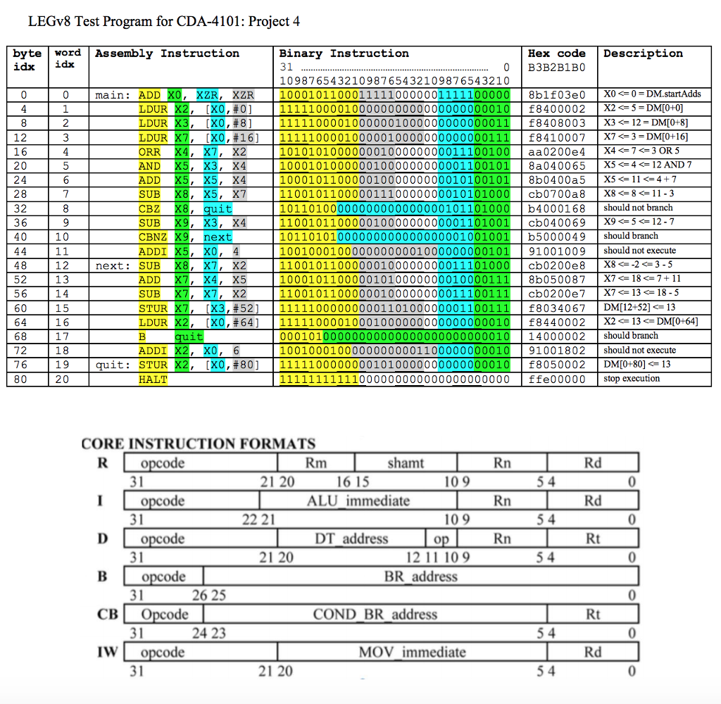
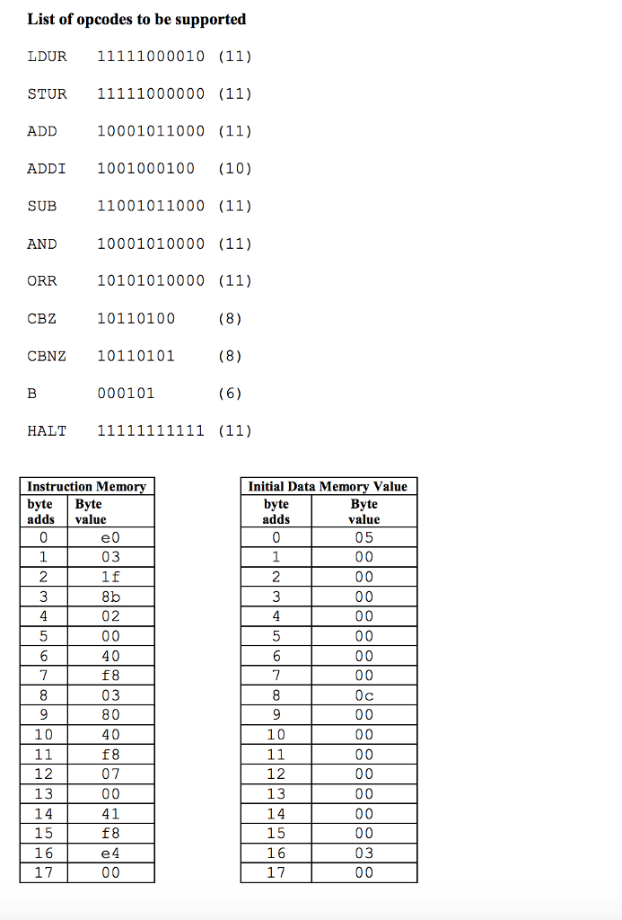
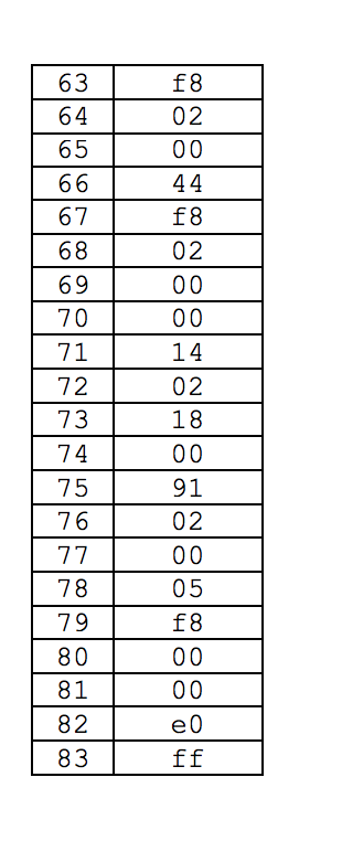
Instruction memory byte values file e0 03 1f 8b 02 00 40 f8 03 80 40 f8 07 00 41 f8 e4 00 02 aa


Instruction memory byte values file e0 03 1f 8b 02 00 40 f8 03 80 40 f8 07 00 41 f8 e4 00 02 aa 65 00 04 8a a5 00 04 8b a8 00 07 cb 68 01 00 b4 69 00 04 cb 49 00 00 b5 09 10 00 91 e8 00 02 cb 87 00 05 8b e7 00 02 cb 67 40 03 f8 02 00 44 f8 02 00 00 14 02 18 00 91 02 00 05 f8 00 00 e0 ff
Initial data memory byte values file
05 00 00 00 00 00 00 00 0c 00 00 00 00 00 00 00 03 00 00 00 00 00 00 00 00 00 00 00 00 00 00 00 00 00 00 00 00 00 00 00
Template test bench verilog code
module template_tb; // processor test bench template reg [7:0] IMem[4095:0]; // 4096 bytes (1024 words) reg [7:0] DMem[8191:0]; // 8192 bytes (1024 double words) reg [31:0] instruction; // all instructions are 32-bit wide reg [63:0] PC; // PC contains 64-bit byte address initial // load instruction memory and data memory begin $readmemh("IM_Bytes.txt", IMem); $readmemh("DM_Bytes.txt", DMem); PC Design a single-cyle processor with necessary combinational logic circuits and sequential logic circuits in Verilog strategy as below: The design should meet all requirements shown in ZyBook Figure 5.4.10 (COD Figure 4.23) Define the instruction memory as 1024 words of 32bits each and the data memory as 1024 words of 64bits each. Use Verilog code given in Section 5.13 and modify it for ARMv8 and include a test bench module. For the processor design, include a design description. Design a single-cyle processor with necessary combinational logic circuits and sequential logic circuits in Verilog strategy as below: The design should meet all requirements shown in ZyBook Figure 5.4.10 (COD Figure 4.23) Define the instruction memory as 1024 words of 32bits each and the data memory as 1024 words of 64bits each. Use Verilog code given in Section 5.13 and modify it for ARMv8 and include a test bench module. For the processor design, include a design description Step by Step Solution
There are 3 Steps involved in it
Step: 1

Get Instant Access to Expert-Tailored Solutions
See step-by-step solutions with expert insights and AI powered tools for academic success
Step: 2

Step: 3

Ace Your Homework with AI
Get the answers you need in no time with our AI-driven, step-by-step assistance
Get Started


