 Just need the deliverables!!
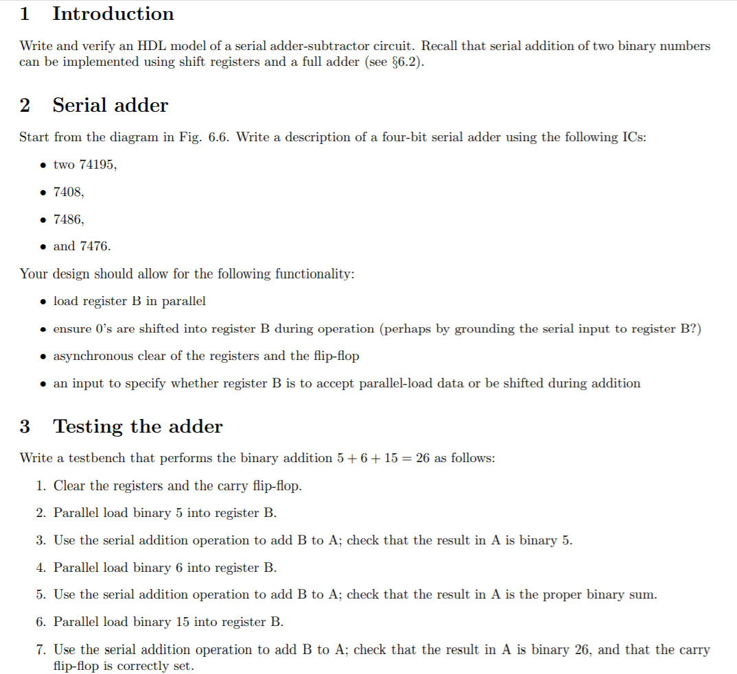
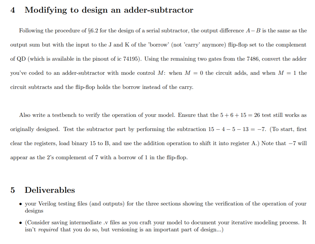
1 Introduction Write and verify an HDL model of a serial adder-subtractor circuit. Recall that serial addition of two binary numbers can be implemented using shift registers and a full adder (see $6.2). 2 Serial adder Start from the diagram in Fig. 6.6. Write a description of a four-bit serial adder using the following ICs: two 74195, 7408, 7486, and 7476. Your design should allow for the following functionality: load register B in parallel ensure I's are shifted into register B during operation (perhaps by grounding the serial input to register B?) asynchronous clear of the registers and the flip-flop an input to specify whether register B is to accept parallel-load data or be shifted during addition 3 Testing the adder Write a testbench that performs the binary addition 5 + 6 + 15 = 26 as follows: 1. Clear the registers and the carry flip-flop. 2. Parallel load binary 5 into register B. 3. Use the serial addition operation to add B to A; check that the result in A is binary 5. 4. Parallel load binary 6 into register B. 5. Use the serial addition operation to add B to A; check that the result in A is the proper binary sum. 6. Parallel load binary 15 into register B. 7. Use the serial addition operation to add B to A; check that the result in A is binary 26, and that the carry flip-flop is correctly set. 4 Modifying to design an adder-subtractor Following the procedure of $6.2 for the design of a serial subtractor, the output difference A-B is the same as the output sum but with the input to the J and K of the 'borrow' (not 'carry' anymore) flip-flop set to the complement of QD (which is available in the pinout of ic 74195). Using the remaining two gates from the 7486, convert the adder you've coded to an adder-subtractor with mode control M: when M = 0 the circuit adds, and when M = 1 the circuit subtracts and the flip-flop holds the borrow instead of the carry. Also write a testbench to verify the operation of your model. Ensure that the 5+6 + 15 = 26 test still works as originally designed. Test the subtractor part by performing the subtraction 15 4-5 13 = -7. (To start, first clear the registers, load binary 15 to B, and use the addition operation to shift it into register A.) Note that 7 will appear as the 2's complement of 7 with a borrow of 1 in the flip-flop. 5 Deliverables your Verilog testing files (and outputs) for the three sections showing the verification of the operation of your designs (Consider saving intermediate .v files as you craft your model to document your iterative modeling process. It isn't required that you do so, but versioning is an important part of design...) 1 Introduction Write and verify an HDL model of a serial adder-subtractor circuit. Recall that serial addition of two binary numbers can be implemented using shift registers and a full adder (see $6.2). 2 Serial adder Start from the diagram in Fig. 6.6. Write a description of a four-bit serial adder using the following ICs: two 74195, 7408, 7486, and 7476. Your design should allow for the following functionality: load register B in parallel ensure I's are shifted into register B during operation (perhaps by grounding the serial input to register B?) asynchronous clear of the registers and the flip-flop an input to specify whether register B is to accept parallel-load data or be shifted during addition 3 Testing the adder Write a testbench that performs the binary addition 5 + 6 + 15 = 26 as follows: 1. Clear the registers and the carry flip-flop. 2. Parallel load binary 5 into register B. 3. Use the serial addition operation to add B to A; check that the result in A is binary 5. 4. Parallel load binary 6 into register B. 5. Use the serial addition operation to add B to A; check that the result in A is the proper binary sum. 6. Parallel load binary 15 into register B. 7. Use the serial addition operation to add B to A; check that the result in A is binary 26, and that the carry flip-flop is correctly set. 4 Modifying to design an adder-subtractor Following the procedure of $6.2 for the design of a serial subtractor, the output difference A-B is the same as the output sum but with the input to the J and K of the 'borrow' (not 'carry' anymore) flip-flop set to the complement of QD (which is available in the pinout of ic 74195). Using the remaining two gates from the 7486, convert the adder you've coded to an adder-subtractor with mode control M: when M = 0 the circuit adds, and when M = 1 the circuit subtracts and the flip-flop holds the borrow instead of the carry. Also write a testbench to verify the operation of your model. Ensure that the 5+6 + 15 = 26 test still works as originally designed. Test the subtractor part by performing the subtraction 15 4-5 13 = -7. (To start, first clear the registers, load binary 15 to B, and use the addition operation to shift it into register A.) Note that 7 will appear as the 2's complement of 7 with a borrow of 1 in the flip-flop. 5 Deliverables your Verilog testing files (and outputs) for the three sections showing the verification of the operation of your designs (Consider saving intermediate .v files as you craft your model to document your iterative modeling process. It isn't required that you do so, but versioning is an important part of design...)
 Just need the deliverables!!


