Answered step by step
Verified Expert Solution
Link Copied!

Question

1 Approved Answer

Lab 4: Design Alternatives Design a circuit to multiply two 2-bit binary numbers, and display the results of the multiplication as a binary number, using

Lab 4: Design Alternatives

Design a circuit to multiply two 2-bit binary numbers, and display the results of the multiplication as a binary number, using as many output bits as necessary. Complete a truth table for the expected output values for the multiplication on the lab data sheet attached. Since this is your first design, you will be given two weeks to complete the lab.

Use Karnaugh maps to simplify the Boolean functions for the outputs, and design realizations of the circuit using.
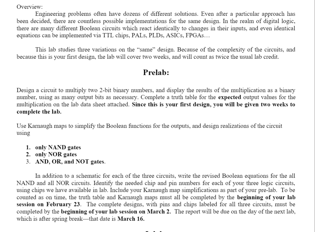
image text in transcribed

Overview: Engineering problems often have dozens of different solutions. Even after a particular approach has been decided, there are countless possible implementations for the same design. In the realm of digital logic, there are many different Boolean circuits which react identically to changes in their inputs, and even identical equations can be implemented via TTL chips, PALs, PLDs, ASICs, FPGAs... This lab studies three variations on the "same" design. Because of the complexity of the circuits, and because this is your first design, the lab will cover two weeks, and will count as twice the usual lab credit. Prelab: Design a circuit to multiply two 2-bit binary numbers, and display the results of the multiplication as a binary number, using as many output bits as necessary. Complete a truth table for the expected output values for the multiplication on the lab data sheet attached. Since this is your first design, you will be given two weeks to complete the lab. Use Karnaugh maps to simplify the Boolean functions for the outputs, and design realizations of the circuit using 1. only NAND gates 2. only NOR gates 3. AND, OR, and NOT gates. In addition to a schematic for each of the three circuits, write the revised Boolean equations for the all NAND and all NOR circuits. Identify the needed chip and pin numbers for each of your three logic circuits, using chips we have available in lab. Include your Karnaugh map simplifications as part of your pre-lab. To be counted as on time, the truth table and Karnaugh maps must all be completed by the beginning of your lab session on February 23. The complete designs, with pins and chips labeled for all three circuits, must be completed by the beginning of your lab session on March 2. The report will be due on the day of the next lab, which is after spring break - that date is March 16

Step by Step Solution

There are 3 Steps involved in it

Step: 1

blur-text-image

Get Instant Access to Expert-Tailored Solutions

See step-by-step solutions with expert insights and AI powered tools for academic success

Step: 2

blur-text-image

Step: 3

blur-text-image

Ace Your Homework with AI

Get the answers you need in no time with our AI-driven, step-by-step assistance

Get Started

Recommended Textbook for

Oracle Databases On The Web Learn To Create Web Pages That Interface With Database Engines

Authors: Robert Papaj, Donald Burleson

11th Edition

1576100995, 978-1576100998

More Books

Students also viewed these Databases questions

Question

6. Vanguard

Answered: 1 week ago

Question

1. PricewaterhouseCoopers

Answered: 1 week ago