Answered step by step
Verified Expert Solution
Question
1 Approved Answer
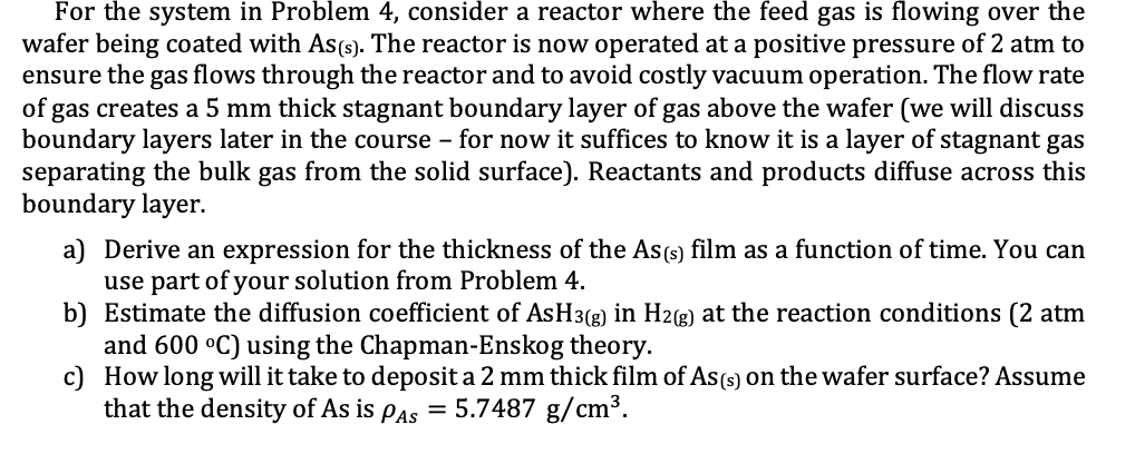
Microelectronic devices are made by depositing many layers of thin films onto silicon wafers. For example, thin films of arsenic for silicon are deposited by
Microelectronic devices are made by depositing many layers of thin films onto silicon wafers. For example, thin films of arsenic for silicon are deposited by chemical vapour deposition CVD of arsine AsH vapour onto the surface of a silicon wafer. The chemical reaction for this CVD process is
AsHg Ass Hg
The process operates at a pressure of Pa and a temperature of oC In many CVD reactors, the gas phase over the thin film is not mixed. Furthermore, at oC the surface reaction is very fast. Consequently, the molecular diffusion of AsH vapour to the surface of the wafer can be assumed to control the rate of Ass formation.
A mixture of arsine and hydrogen gas continuously flows into the reactor at a molar ratio of : H:AsH A diffuser cm above the wafer provides a quiescent gas space over the growing Ass film.

Step by Step Solution
There are 3 Steps involved in it
Step: 1

Get Instant Access to Expert-Tailored Solutions
See step-by-step solutions with expert insights and AI powered tools for academic success
Step: 2

Step: 3

Ace Your Homework with AI
Get the answers you need in no time with our AI-driven, step-by-step assistance
Get Started


