Multi-part Question.
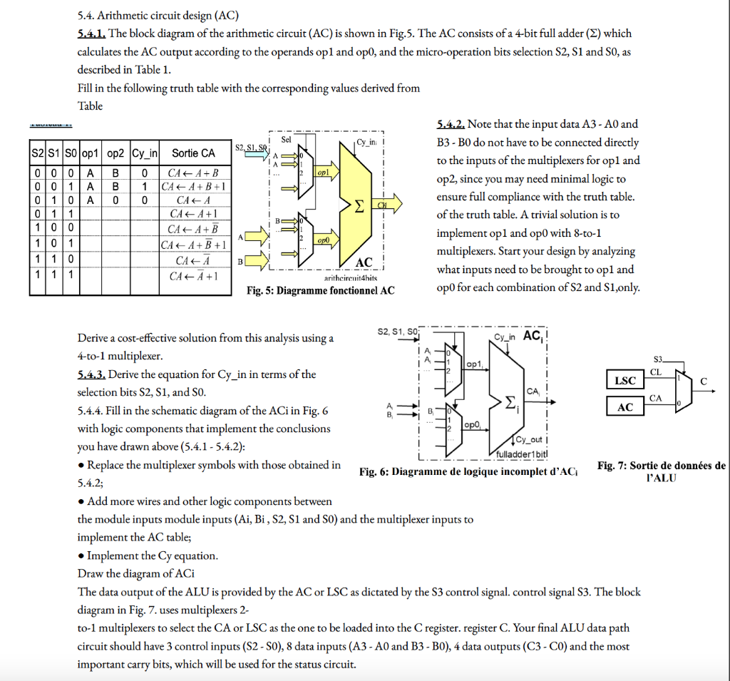
5.4. Arithmetic circuit design (AC) 5.4.1. The block diagram of the arithmetic circuit (AC) is shown in Fig.5. The AC consists of a 4-bit full adder () which calculates the AC output according to the operands op1 and op0, and the micro-operation bits selection S2, S1 and S0, as described in Table 1. Fill in the following truth table with the corresponding values derived from Table Derive a cost-effective solution from this analysis using a 4-to-1 multiplexer. 5.4.2. Note that the input data A3 - A0 and B3 - B0 do not have to be connected directly to the inputs of the multiplexers for op1 and op2, since you may need minimal logic to ensure full compliance with the truth table. of the truth table. A trivial solution is to implement op1 and op0 with 8-to-1 multiplexers. Start your design by analyzing what inputs need to be brought to op1 and op0 for each combination of S2 and S1,only. 5.4.3. Derive the equation for Cy_in in terms of the selection bits S2, S1, and S0. 5.4.4. Fill in the schematic diagram of the ACi in Fig. 6 with logic components that implement the conclusions you have drawn above (5.4.1-5.4.2): - Replace the multiplexer symbols with those obtained in Fig. 6: Diagramme de logique incomplet d'AC Fig. 7: Sortie de donnes de 5.4.2; - Add more wires and other logic components between the module inputs module inputs ( Ai,Bi,S2,S1 and S0) and the multiplexer inputs to implement the AC table; - Implement the Cy equation. Draw the diagram of ACi The data output of the ALU is provided by the AC or LSC as dictated by the S3 control signal. control signal S3. The block diagram in Fig. 7. uses multiplexers 2- to-1 multiplexers to select the CA or LSC as the one to be loaded into the C register. register C. Your final ALU data path circuit should have 3 control inputs (S2 - S0), 8 data inputs (A3 - A0 and B3 - B0), 4 data outputs (C3 - C0) and the most important carry bits, which will be used for the status circuit. 5.4. Arithmetic circuit design (AC) 5.4.1. The block diagram of the arithmetic circuit (AC) is shown in Fig.5. The AC consists of a 4-bit full adder () which calculates the AC output according to the operands op1 and op0, and the micro-operation bits selection S2, S1 and S0, as described in Table 1. Fill in the following truth table with the corresponding values derived from Table Derive a cost-effective solution from this analysis using a 4-to-1 multiplexer. 5.4.2. Note that the input data A3 - A0 and B3 - B0 do not have to be connected directly to the inputs of the multiplexers for op1 and op2, since you may need minimal logic to ensure full compliance with the truth table. of the truth table. A trivial solution is to implement op1 and op0 with 8-to-1 multiplexers. Start your design by analyzing what inputs need to be brought to op1 and op0 for each combination of S2 and S1,only. 5.4.3. Derive the equation for Cy_in in terms of the selection bits S2, S1, and S0. 5.4.4. Fill in the schematic diagram of the ACi in Fig. 6 with logic components that implement the conclusions you have drawn above (5.4.1-5.4.2): - Replace the multiplexer symbols with those obtained in Fig. 6: Diagramme de logique incomplet d'AC Fig. 7: Sortie de donnes de 5.4.2; - Add more wires and other logic components between the module inputs module inputs ( Ai,Bi,S2,S1 and S0) and the multiplexer inputs to implement the AC table; - Implement the Cy equation. Draw the diagram of ACi The data output of the ALU is provided by the AC or LSC as dictated by the S3 control signal. control signal S3. The block diagram in Fig. 7. uses multiplexers 2- to-1 multiplexers to select the CA or LSC as the one to be loaded into the C register. register C. Your final ALU data path circuit should have 3 control inputs (S2 - S0), 8 data inputs (A3 - A0 and B3 - B0), 4 data outputs (C3 - C0) and the most important carry bits, which will be used for the status circuit