Question
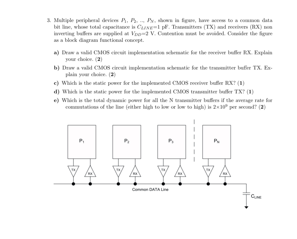
Multiple peripheral devices P_(1),P_(2),..,P_(N) , shown in figure, have access to a common data bit line, whose total capacitance is C_(LINE)=1pF . Transmitters (TX) and
Multiple peripheral devices
P_(1),P_(2),..,P_(N), shown in figure, have access to a common data bit line, whose total capacitance is
C_(LINE)=1pF. Transmitters (TX) and receivers (RX) non inverting buffers are supplied at
V_(DD)=2V. Contention must be avoided. Consider the figure as a block diagram functional concept.\ a) Draw a valid CMOS circuit implementation schematic for the receiver buffer RX. Explain your choice. \ b) Draw a valid CMOS circuit implementation schematic for the transmitter buffer TX. Explain your choice. \ c) Which is the static power for the implemented CMOS receiver buffer RX? \ d) Which is the static power for the implemented CMOS transmitter buffer TX? \ e) Which is the total dynamic power for all the
Ntransmitter buffers if the average rate for commutations of the line (either high to low or low to high) is
2\\\\times 10^(9)per second?

Step by Step Solution
There are 3 Steps involved in it
Step: 1

Get Instant Access to Expert-Tailored Solutions
See step-by-step solutions with expert insights and AI powered tools for academic success
Step: 2

Step: 3

Ace Your Homework with AI
Get the answers you need in no time with our AI-driven, step-by-step assistance
Get Started


