Answered step by step
Verified Expert Solution
Question
1 Approved Answer
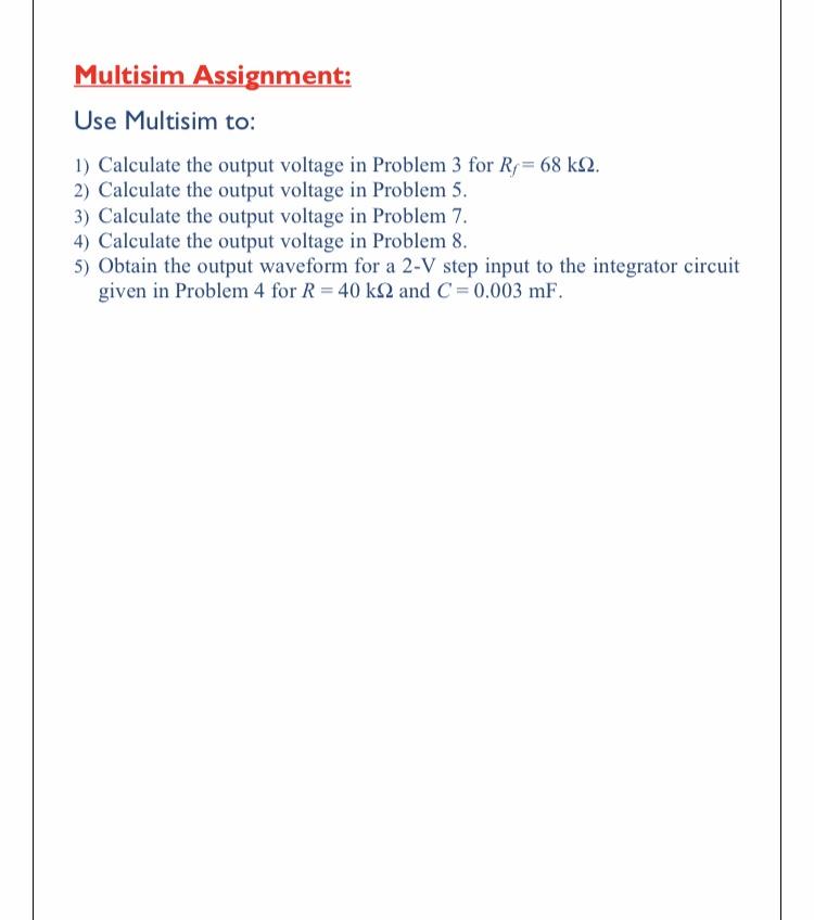
Multisim Assignment: Use Multisim to: 1) Calculate the output voltage in Problem 3 for R= 68 k2. 2) Calculate the output voltage in Problem


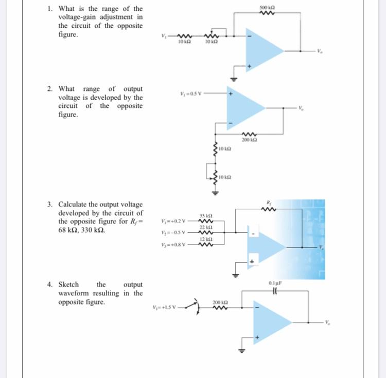
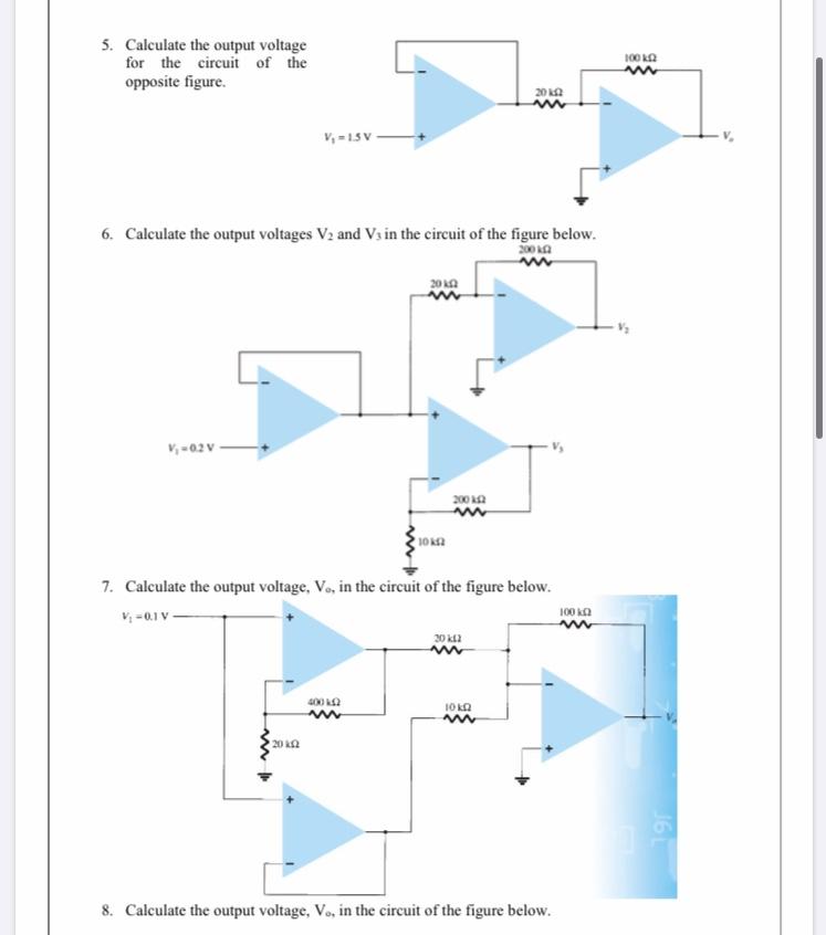
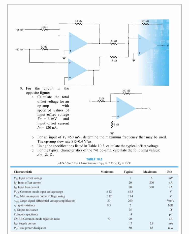
Multisim Assignment: Use Multisim to: 1) Calculate the output voltage in Problem 3 for R= 68 k2. 2) Calculate the output voltage in Problem 5. 3) Calculate the output voltage in Problem 7. 4) Calculate the output voltage in Problem 8. 5) Obtain the output waveform for a 2-V step input to the integrator circuit given in Problem 4 for R = 40 k2 and C= 0.003 mF. 1. What is the range of the voltage-gain adjustment in the circuit of the opposite figure. S00 ka 10 kn 10 ka 2. What range of output voltage is developed by the circuit of the opposite figure. V, 0s v- 200 ka 10 k 10 2 3. Calculate the output voltage developed by the circuit of the opposite figure for Ry = 68 k2, 330 k2. 33 ka V-0.2 V V-05 V 22 ka 12 kl 4. Sketch waveform resulting in the opposite figure. the output 200 k2 V= +15 V 5. Calculate the output voltage for the circuit of the opposite figure. 100 kA 20 k2 V, = 15 V 6. Calculate the output voltages V2 and Vs in the circuit of the figure below. 200 ka 20 kA V, -02 V 200 Aa 7. Calculate the output voltage, Vo, in the eircuit of the figure below. V -0.1 V- 100 ka 20 ka 400 k2 10 ka 20 2 8. Calculate the output voltage, Vo, in the circuit of the figure below. 161 600 kS2 15 kN -25 mV 30 k2 30 kl2 -20 mV 15 K2 9. For the circuit in the opposite figure: a. Calculate the total 200 k2 V, M offset voltage for an with op-amp specified values of input offset voltage Vio = 6 mV input offset current Ijo = 120 nA. and 2 k2 b. For an input of V =50 mV, determine the maximum frequency that may be used. The op-amp slew rate SR=0.4 V/us. c. Using the specifications listed in Table 10.3, calculate the typical offset voltage. d. For the typical characteristics of the 741 op-amp, calculate the following values: Ac, Z. Z. TABLE 10.3 HA741 Electrical Characteristics: Vee 1S V, TA 25C Characteristic Minimum Typical Maximum Unit Vio Input offset voltage ho Input offset current In Input bias current Vicr Common-mode input voltage range VOM Maximum peak output voltage swing Avp Large-signal differential voltage amplification , Input resistance , Output resistance G, Input capacitance CMRR Common-mode rejection ratio mV 20 200 nA 80 500 nA 212 213 V 112 14 V 20 200 V/mV 0.3 2 M 75 1.4 pF 70 90 dB 1.7 Ice Supply current Pp Total 2.8 mA power dissipation 50 85 mW
Step by Step Solution
★★★★★
3.42 Rating (171 Votes )
There are 3 Steps involved in it
Step: 1
1Vo33998...
Get Instant Access to Expert-Tailored Solutions
See step-by-step solutions with expert insights and AI powered tools for academic success
Step: 2

Step: 3

Ace Your Homework with AI
Get the answers you need in no time with our AI-driven, step-by-step assistance
Get Started


