

Question: need help! using vivado **Edited with better resol. Assignment 3: Multi-cycle Processor Design and Simulation For this assignment, you need to describe the multi-cycle processor
need help! using vivado **Edited with better resol.
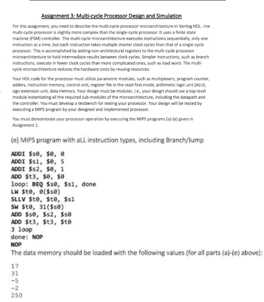
Assignment 3: Multi-cycle Processor Design and Simulation For this assignment, you need to describe the multi-cycle processor microarchitecture in Verilog HDL. The multi-cycle processor is slightly more complex than the single-cycle processor. It uses a finite state machine (FSM) controller. The multi-cycle microarchitecture executes instructions sequentially, only one instruction at a time, but each instruction takes multiple shorter clock cycles than that of a single-cycle processor. This is accomplished by adding non-architectural registers to the multi-cycle processor microarchitecture to hold intermediate results between clock cycles. Simpler instructions, such as branch instructions, execute in fewer clock cycles than more complicated ones, such as load word. The multi- cycle microarchitecture reduces the hardware costs by reusing resources. Your HDL code for the processor must utilize parametric modules, such as multiplexers, program counter, adders, instruction memory, control unit, register file in the read-first mode, arithmetic logic unit (ALU), sign extension unit, data memory. Your design must be modular, i.e., your design should use a top-level module instantiating all the required sub-modules of the microarchitecture, including the datapath and the controller. You must develop a testbench for testing your processor. Your design will be tested by executing a MIPS program by your designed and implemented processor. You must demonstrate your processor operation by executing the MIPS programs (a)-(e) given in Assignment 1. (e) MIPS program with all instruction types, including Branch/Jump ADDI $se, se, e ADDI $51, $e, 5 ADDI $52, $e, 1 ADD $t3, $8, $8 loop: BEQ $se, $si, done LW Sto, ($se) SLLV $te, Ste, $s1 SW Sto, 31($se) ADD $se, $s2, $s@ ADD $t3, $t3, $te 3 loop done: NOP NOP The data memory should be loaded with the following values (for all parts (a)-(e) above): 17 31 -5 250 Assignment 3: Multi-cycle Processor Design and Simulation For this assignment, you need to describe the multi-cycle processor microarchitecture in Verilog HDL. The multi-cycle processor is slightly more complex than the single-cycle processor. It uses a finite state machine (FSM) controller. The multi-cycle microarchitecture executes instructions sequentially, only one instruction at a time, but each instruction takes multiple shorter clock cycles than that of a single-cycle processor. This is accomplished by adding non-architectural registers to the multi-cycle processor microarchitecture to hold intermediate results between clock cycles. Simpler instructions, such as branch instructions, execute in fewer clock cycles than more complicated ones, such as load word. The multi- cycle microarchitecture reduces the hardware costs by reusing resources. Your HDL code for the processor must utilize parametric modules, such as multiplexers, program counter, adders, instruction memory, control unit, register file in the read-first mode, arithmetic logic unit (ALU), sign extension unit, data memory. Your design must be modular, i.e., your design should use a top-level module instantiating all the required sub-modules of the microarchitecture, including the datapath and the controller. You must develop a testbench for testing your processor. Your design will be tested by executing a MIPS program by your designed and implemented processor. You must demonstrate your processor operation by executing the MIPS programs (a)-(e) given in Assignment 1. (e) MIPS program with all instruction types, including Branch/Jump ADDI $se, se, e ADDI $51, $e, 5 ADDI $52, $e, 1 ADD $t3, $8, $8 loop: BEQ $se, $si, done LW Sto, ($se) SLLV $te, Ste, $s1 SW Sto, 31($se) ADD $se, $s2, $s@ ADD $t3, $t3, $te 3 loop done: NOP NOP The data memory should be loaded with the following values (for all parts (a)-(e) above): 17 31 -5 250
Step by Step Solution
There are 3 Steps involved in it

Get step-by-step solutions from verified subject matter experts