Answered step by step
Verified Expert Solution
Question
1 Approved Answer
Need help with the following step signal mapping in VHDL this line of code: -- RegDst Step 1: Building control circuit (mips.vhd) . Implement the

Need help with the following step signal mapping in VHDL this line of code:
-- RegDst
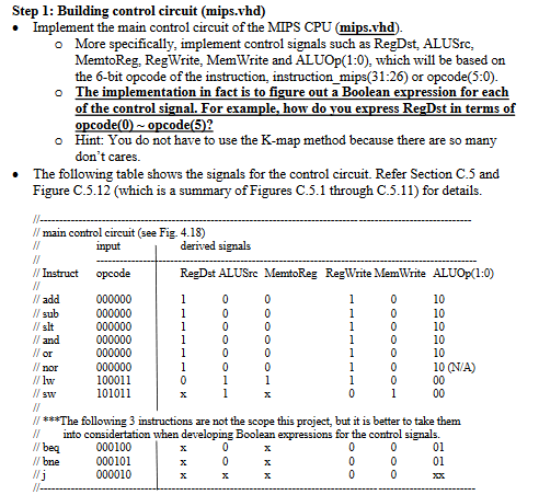
Step 1: Building control circuit (mips.vhd) . Implement the main control circuit of the MIPS CPU (mips.vhd). More specifically, implement control signals such as RegDst, ALUSrc, MemtoReg, RegWrite, MemWrite and ALUOp(1:0), which will be based on the 6-bit opcode of the instruction, instruction mips(31:26) or opcode(5:0). The implementation in fact is to figure out a Boolean expression for each of the control signal. For example, how dov o o ress RegDst in terms of code(0) opcode(5)? o Hint: You do not have to use the K-map method because there are so many don't cares. The following table shows the signals for the control circuit. Refer Section C.5 and Figure C.5.12 (which is a summary of Figures C.5.1 through C.5.11) for details. . main control circuit (see Fig. 4.13) derived signals Instruct opcode RegDst ALUSrc MemtoReg RegWrite MemWrite ALUOp 1:0) add / sub / slt and 10 10 10 10 10 N/A) lw 100011 101011 *The following 3 instructions are not the scope this project, but it is better to take them into considertation when developing Boolean expressions for the control signals. l beq / bne 000100 000101 000010 2 0 Step 1: Building control circuit (mips.vhd) . Implement the main control circuit of the MIPS CPU (mips.vhd). More specifically, implement control signals such as RegDst, ALUSrc, MemtoReg, RegWrite, MemWrite and ALUOp(1:0), which will be based on the 6-bit opcode of the instruction, instruction mips(31:26) or opcode(5:0). The implementation in fact is to figure out a Boolean expression for each of the control signal. For example, how dov o o ress RegDst in terms of code(0) opcode(5)? o Hint: You do not have to use the K-map method because there are so many don't cares. The following table shows the signals for the control circuit. Refer Section C.5 and Figure C.5.12 (which is a summary of Figures C.5.1 through C.5.11) for details. . main control circuit (see Fig. 4.13) derived signals Instruct opcode RegDst ALUSrc MemtoReg RegWrite MemWrite ALUOp 1:0) add / sub / slt and 10 10 10 10 10 N/A) lw 100011 101011 *The following 3 instructions are not the scope this project, but it is better to take them into considertation when developing Boolean expressions for the control signals. l beq / bne 000100 000101 000010 2 0
Step by Step Solution
There are 3 Steps involved in it
Step: 1

Get Instant Access to Expert-Tailored Solutions
See step-by-step solutions with expert insights and AI powered tools for academic success
Step: 2

Step: 3

Ace Your Homework with AI
Get the answers you need in no time with our AI-driven, step-by-step assistance
Get Started


