Answered step by step
Verified Expert Solution
Question
1 Approved Answer
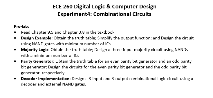
Need the prelab for this any that you can do will be appreciated. ECE 260 Digital Logic & Computer Desigrn Experiment4: Combinational Circuits Pre-lab: Read


Need the prelab for this any that you can do will be appreciated.
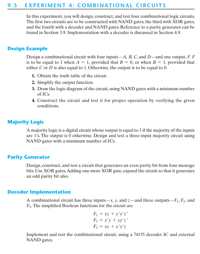
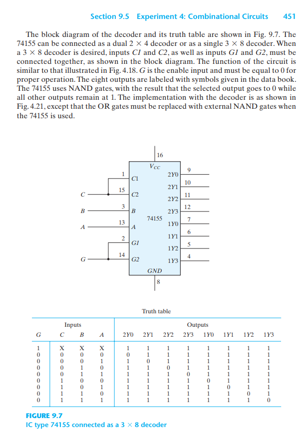
ECE 260 Digital Logic & Computer Desigrn Experiment4: Combinational Circuits Pre-lab: Read Chapter 9.5 and Chapter 3.8 in the textbook Design Example: Obtain the truth table; Simplify the output function; and Design the circuit using NAND gates with minimum number of ICs. Majority Logic: Obtain the truth table; Design a three-input majority circuit using NANDs with a minimum number of ICs Parity Generator: Obtain the truth table for an even parity bit generator and an odd parity bit generator; Design the circuits for the even parity bit generator and the odd parity bit generator, respectively Decoder Implementation: Design a 3-input and 3-output combinational logic circuit using a decoder and external NAND gates 9.5 EXPERIMENT 4: COMBINATIONAL CIRCUITS In this experiment, you will design, construct, and test four combinational logic circuits. The first two circuits are to be constructed with NAND gates, the third with XOR gates, and the fourth with a decoder and NAND gates. Reference to a parity generator can be found in Section 3.9. Implementation with a decoder is discussed in Section 4.9 Design Example Design a combinational circuit with four inputs-A, B, C,and D-and one output, F.F is to be equal to 1 when A 1, provided that B0, or when B-1, provided that either C or D is also equal to 1. Otherwise, the output is to be equal to 0 1. Obtain the truth table of the circuit. 2. Simplify the output function. 3. Draw the logic diagram of the circuit, using NAND gates with a minimum number of ICs. 4. Construct the circuit and test it for proper operation by verifying the given conditions. Majority Logic A majority logic is a digital circuit whose output is equal to 1 if the majority of the inputs are 1's. The output is 0 otherwise. Design and test a three-input majority circuit using NAND gates with a minimum number of ICs. Parity Generator Design, construct, and test a circuit that generates an even parity bit from four message bits. Use XOR gates. Adding one more XOR gate, expand the circuit so that it generates an odd parity bit also. Decoder Implementation A combinational circuit has three inputs-x, y, and z-and three outputs-Fi, F2, and F3. The simplified Boolean functions for the circuit are F, = xz + x,y, z' F3xy x'y'z Implement and test the combinational circuit, using a 74155 decoder IC and external NAND gates. 451 Section 9.5 Experiment 4: Combinational Circuits The block diagram of the decoder and its truth table are shown in Fig. 9.7. The 74155 can be connected as a dual 2 X 4 decoder or as a single 3 X 8 decoder. When a 3 X 8 decoder is desired, inputs C1 and C2, as well as inputs GI and G2, must be connected together, as shown in the block diagram. The function of the circuit is similar to that illustrated in Fig. 4.18. G is the enable input and must be equal to 0 for proper operation. The eight outputs are labeled with symbols given in the data book The 74155 uses NAND gates, with the result that the selected output goes to 0 while all other outputs remain at 1. The implementation with the decoder is as shown in Fig. 4.21, except that the OR gates must be replaced with external NAND gates when the 74155 is used 16 2YO 2Y1 2Y2 2Y3 C1 10 15 C2 12 B 14155 1Y0 13 1Y1 1Y2 1Y3 G1 14 G2 GND Truth table Inputs Outputs 2YO 2Y1 2Y2 2Y3 1YO 1Y1 1Y21Y3 FIGURE 9.7 IC type 74155 connected as a3X 8 decoderStep by Step Solution
There are 3 Steps involved in it
Step: 1

Get Instant Access to Expert-Tailored Solutions
See step-by-step solutions with expert insights and AI powered tools for academic success
Step: 2

Step: 3

Ace Your Homework with AI
Get the answers you need in no time with our AI-driven, step-by-step assistance
Get Started


