

Answered step by step
Verified Expert Solution
Question
1 Approved Answer
page 13 and 14 are included. Please show work and don't copy wrong answer. If it is correct, I will give thumbs up! Thank you!
page 13 and 14 are included.
Please show work and don't copy wrong answer. If it is correct, I will give thumbs up! Thank you!
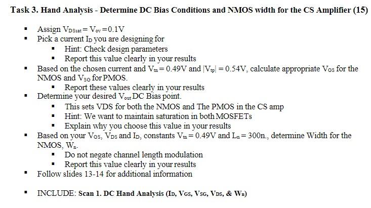
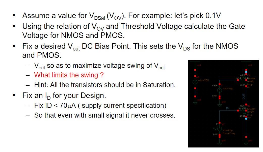
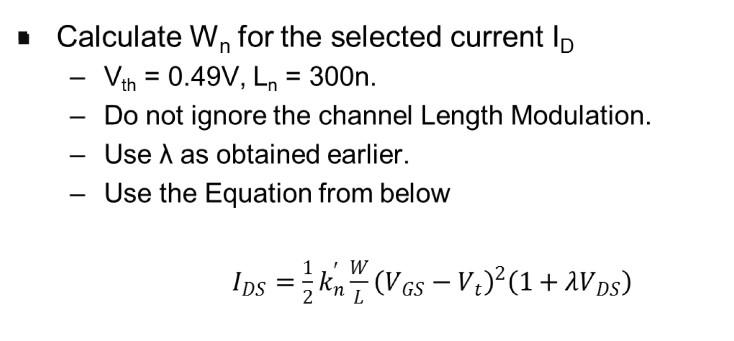
. Task 3. Hand Analysis - Determine DC Bias Conditions and NMOS width for the CS Amplifier (15) Assign VDSsat = Vor=0.1V Pick a current In you are designing for Hint: Check design parameters Report this value clearly in your results Based on the chosen current and Von = 0.49V and Vip = 0.54V, calculate appropriate Ves for the NMOS and Vsg for PMOS. Report these values clearly in your results Determine your desired Vout DC Bias point. This sets VDS for both the NMOS and The PMOS in the CS amp Hint: We want to maintain saturation in both MOSFETS Explain why you choose this value in your results Based on your Vos, Vps and ID, constants Vt = 0.49V and La = 300n., determine Width for the NMOS, W.- Do not negate channel length modulation Report this value clearly in your results Follow slides 13-14 for additional information 1 1 INCLUDE: Scan 1. DC Hand Analysis (ID, VG, VG, VDs, & Wn) 1 Assume a value for Vosat (Vov). For example: let's pick 0.1V Using the relation of Voy and Threshold Voltage calculate the Gate Voltage for NMOS and PMOS. Fix a desired Vout DC Bias Point. This sets the Vos for the NMOS and PMOS. - Vout so as to maximize voltage swing of Vou What limits the swing? Hint: All the transistors should be in Saturation. Fix an lo for your Design. Fix IDStep by Step Solution
There are 3 Steps involved in it
Step: 1

Get Instant Access to Expert-Tailored Solutions
See step-by-step solutions with expert insights and AI powered tools for academic success
Step: 2

Step: 3
Ace Your Homework with AI
Get the answers you need in no time with our AI-driven, step-by-step assistance
Get Started
Advanced Level Audit Q And A 2014
Authors: ACA Simplified
1st Edition
1500852538, 978-1500852535