

Question: Phase 1: 32-bit ALU simulation Write a simulation code for the 32-bit ALU described in the attached figures. The ALU uses 32-bit ripple-carry adder, and
Phase 1: 32-bit ALU simulation
Write a simulation code for the 32-bit ALU described in the attached figures.
The ALU uses 32-bit ripple-carry adder, and performs six operations, i.e., logic AND,
logic OR, addition, subtraction, set on less than (slt), and logic NOR.
In addition to the result (32 bits wide), the ALU should also return signals for overflow
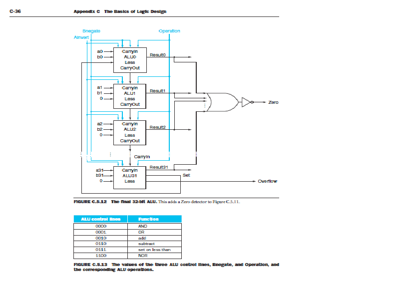
(1 bit) and zero (1 bit) as shown in Figure C.5.12.
Step 1
As the first step, write a simulation code for a basic component 1-bit ALU, which performs 1-
bit operations for the above six operations.
In the 1-bit ALU, there are five sub-components to simulate, which are AND-gate, OR-gate,
1-bit full adder, 2x1_Mux, and 4x1_MUX. //you dont have to simulate the negator.
Each sub-component should be implemented as a function with input/output parameters.
Component 1-bit ALU should also be implemented as a function with input/output parameters.
As shown in Figure C.5.12, there are 7 inputs and 2 outputs for each 1-bit ALU, except the last
one, which has two extra outputs (overflow and set signals).
You should write an extra simulation module (a function) for the last 1-bit ALU.
Test your 1-bit ALU with your own test data.
Step 2
Extend your simulation code designed in Step 1 for the 32-bit ALU. The complete structure
is depicted in Figure- C.5.12.
Data A(a0-a31) and B(b0-b31) are 32 bits each, and you can store them in two 32-bit integer vars.
You can assign values to A and B using decimal, binary, or hexadecimal format, e.g.,
int A = 0x1234abcd; //value in hexadecimal format
Manipulation of the 32-bit data in your simulator is up to you, e.g., using bit-wise operations
or array of 32 symbols (1 or 0 each), etc.
Based on the control signals (total 4 bits, as shown in Figure C.5.13) and input data (A and
B, each 32 bits), your 32-bit ALU should generate appropriate outputs.
Test data for simulation program phase1
Test your simulator with the following data sets:
int a = 0x00000003; //Hex number assignment (decimal 3)
int b = 0x00000004; //Hex number assignment (decimal 4)
int a = 0xffffffb7 //Hex number assignment (decimal -73)
int b = 0x00000046 //Hex number assignment (decimal 70)
Test for all the operations, i.e., AND, OR, ADD, SUB, SLT, and NOR.
Phase 2: MIPS multi-cycled CPU (datapath & control) simulation
Write a simulation code for the multi-cycled implementation of the MIPS architecture.
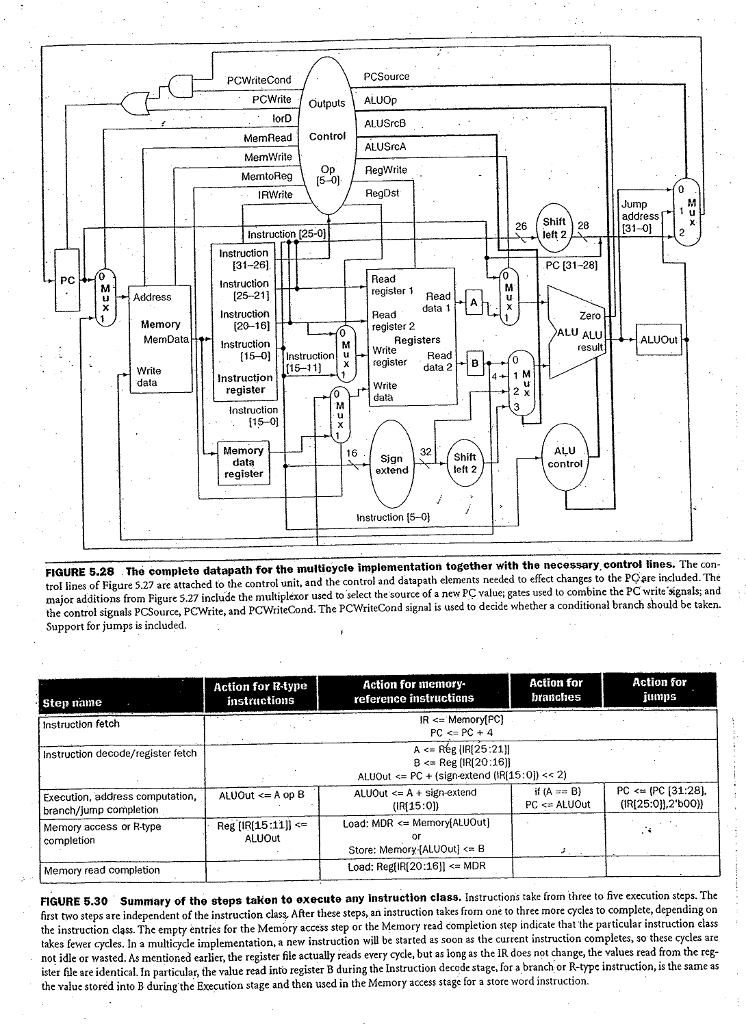
The multi-cycled datapath with control signals is illustrated in Figure 5.28 (attached) and
micro operations of each cycle are shown in Figure 5.30 (attached).
The datapath uses only one ALU since multiple execution steps for an instruction share it
in different clock cycles. You should use the 32-bit ALU simulation module, which was
built in the phase 1.
In each clock cycle, appropriate control signals are generated to control needed components
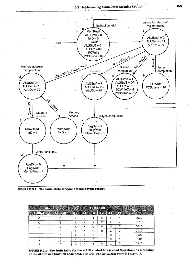
in the datapath. You should use the FSM-based control a state diagram of the FSM is
shown in Figure D.3.1 (attached).
Major components in the simulation
Memory: Memory consists of both instructions and data. In the simulation, use a
simplified memory module that starts from byte address 0hex and ends with
byte address C7hex (199dec). Assume that the instruction starts from byte
address 0hex and the data starts from byte address 64hex (100dec).
Register file: There are 32 registers in the register file.
In the simulation code, you should prepare a table with two fields, i.e.,
register_number and 32-bit content.
32-bit ALU: the one you designed in Phase 1; it should handle 6 operations
(AND, OR, Add, Sub, Slt, NOR) and also generate Zero and Overflow output (1/0).
Special/Intermediate Registers: each 32-bits long
PC (Program Counter)
IR (Instruction Rgister)
MDR (Memory Data Register): for load instruction
A: operand1 for ALU
B: operand2 for ALU
ALUout: result from ALU
Other Components:
Mux-1: Selects memory address for instruction (PC) or data (ALUout), based on
control signal IorD.
Mux-2: Selects write-register number from rt (for load) and rd (for R-type), based on
the control signal RegDst.
Mux-3: Selects Write-data from ALUout (for R-type) and MDR (for load), based on
the control signal MemtoReg.
Mux-4: Selects ALU operand-1 from PC and A, based on the control signal ALUSrcA.
Mux-5: Selects ALU operand-2 from B, #4 (for PC+4), sign-extended offset (for load/store),
sign-extended&
Mux-6: Selects the next PC value from ALU (PC+4), ALUout (branch target), and
Jump target, based on the 2-bit control signal PCSource.
Sign-extend unit: converts 16-bit number to 32-bit sign-extended number.
Shift-left2 unit: performs
Control Unit
In each clock cycle, the control unit (you should write a simulation module) generates
appropriate control signals and components in the datapath operate based on them.
Instruction Set
Your simulator should handle at least the following subset of MIPS instructions (see lecture note):
Arithmetic: add, sub
Data transfer: lw, sw
Logical: and, or, nor
Conditional branch: beq, bne, slt
Jump: j
-----------------------------------------------------------------------------------------------------------------
Input:
MIPS machine instructions and data for a program is stored in a text file.
Load the instructions into the instruction memory area (starting from byte address 0hex),
and data (if any) into the data memory area (starting from byte address 64hex).
Output:
1. Display the initial configuration; i.e., memory contents with address (0hex ~ C7hex),
and the register file contents (reg. #s and contents)
2. For each clock cycle, display contents of the following intermediate registers;
PC, IR, MDR, A, B, ALUout. //display in binary (32 bits) format
3. Display the final configuration; i.e., memory contents with address (0hex ~ C7hex)
and the register file contents (reg. # and contents).
Simulation project sample testing code
Assumptions: initial value of $gp = 64hex (100dec)
value of $zero = 0
Sample high-level code:
load x;
load y;
while (x
y = y-1;
store y;
Corresponding MIPS assembly code:
lw $t0, 0($gp); x
lw $t1, 4($gp); y
lw $s0, 8($gp); #1
Loop: slt $s1, $t0, $t1; if (t0
beq $s1, $zero, Exit; if s1 ==0, Exit
sub $t1, $t1, $s0; y = y - 1
j Loop;
Exit: sw $t1, 4($gp); store y
Loader format:
8 3
10001111100010000000000000000000
10001111100010010000000000000100
10001111100100000000000000001000
00000001000010011000100000101010
00010010001000000000000000000010
00000001001100000100100000100010
00001000000000000000000000000011
10101111100010010000000000000100
00000000000000000000000000000011
00000000000000000000000000000101
00000000000000000000000000000001
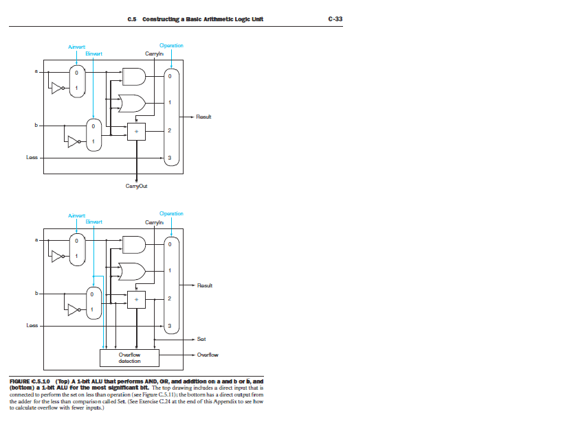
C-33 Oparation Binvert Result nega Oparation Binvart Carryln Rosult Ovarlow RIGURE C.5.10 (Top) A 1-bit ALU that performs AND, OR, amd addition on a and b or b, and conmected to perforn the set on less than operation (see Figrure C5.1the bottorn has a direct output from the adder for the less than comparisonad Set. (See ExenciseC24 atthe end of this Appendix to see how to calculate overflow with fewer inputs.) C-33 Oparation Binvert Result nega Oparation Binvart Carryln Rosult Ovarlow RIGURE C.5.10 (Top) A 1-bit ALU that performs AND, OR, amd addition on a and b or b, and conmected to perforn the set on less than operation (see Figrure C5.1the bottorn has a direct output from the adder for the less than comparisonad Set. (See ExenciseC24 atthe end of this Appendix to see how to calculate overflow with fewer inputs.)
Step by Step Solution
There are 3 Steps involved in it

Get step-by-step solutions from verified subject matter experts