Answered step by step
Verified Expert Solution
Link Copied!

Question

1 Approved Answer

please answer the whole following questions one by one faster Al. Connect the circuit shown in the Fig. 10.1. Then apply the logic levels given
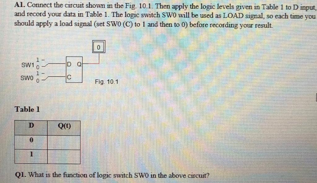
image text in transcribed

image text in transcribedimage text in transcribedimage text in transcribedimage text in transcribedimage text in transcribedimage text in transcribedimage text in transcribedimage text in transcribedplease answer the whole following questions one by one faster

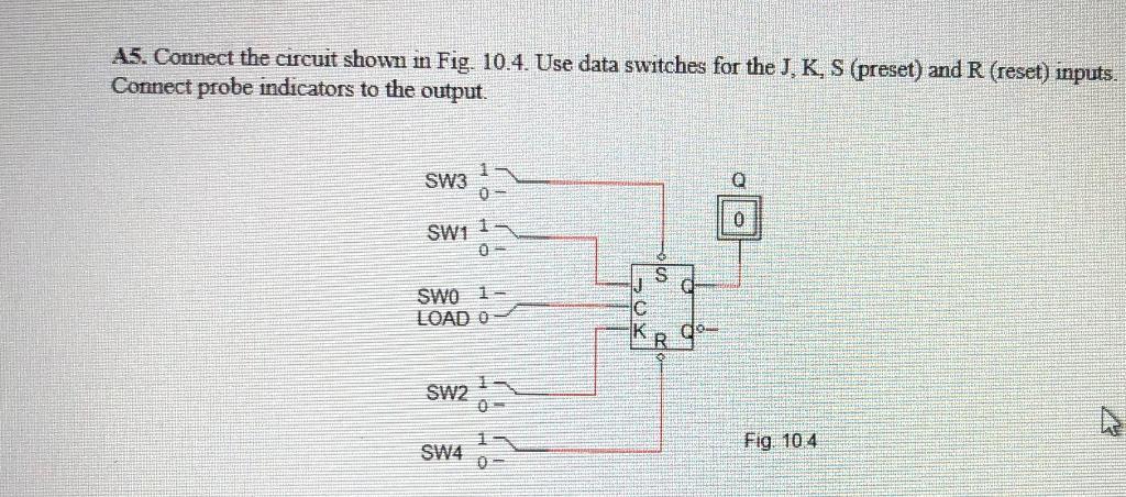
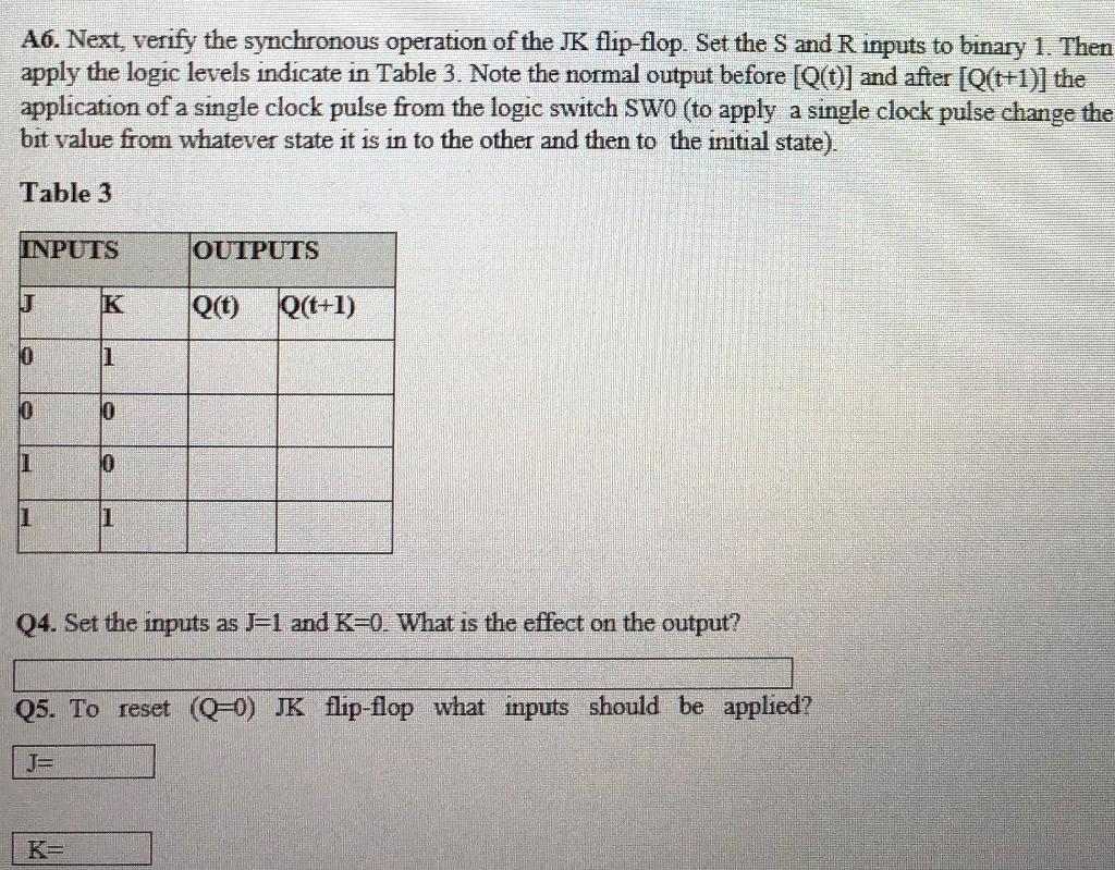
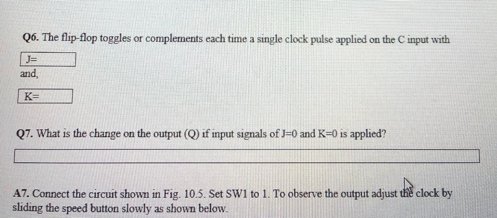
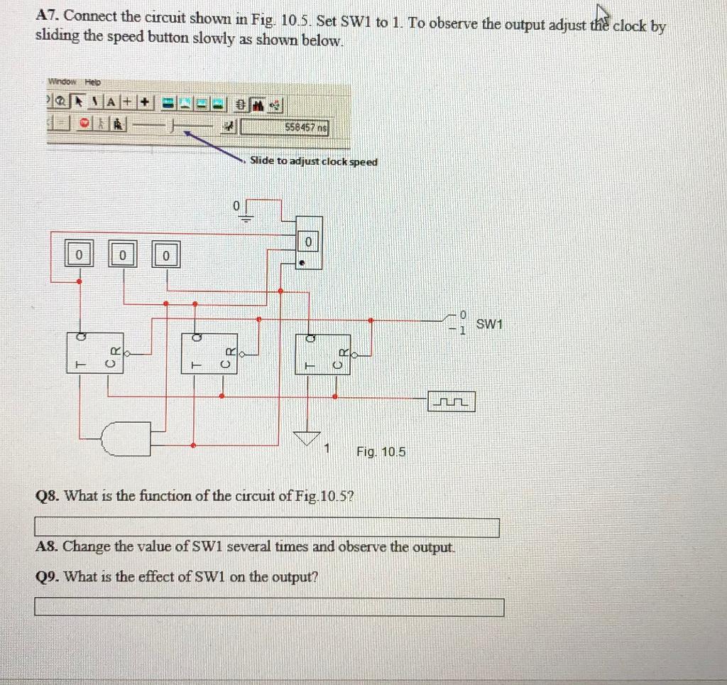
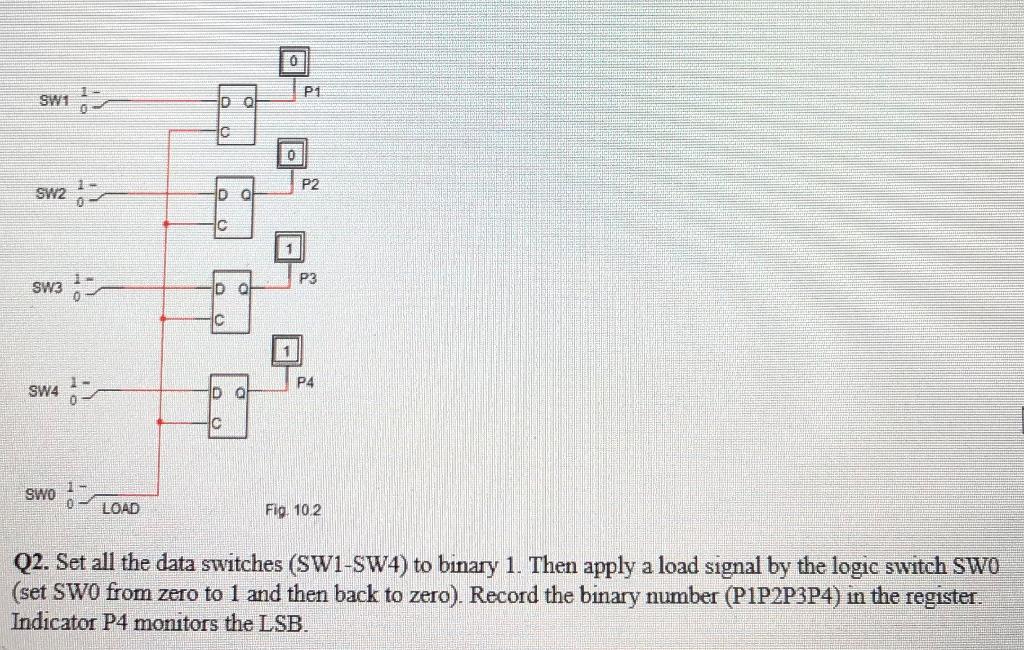
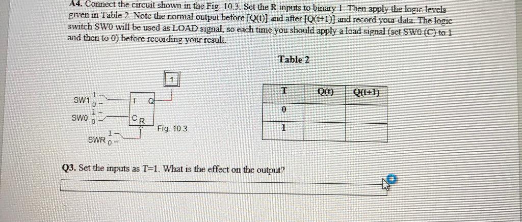
Al. Connect the circuit shown in the Fig. 10.1. Then apply the logic levels given in Table 1 to D input, and record your data in Table 1. The logic switch SWO will be used as LOAD signal, so each time you should apply a load signal (set SWO (C) to 1 and then to 0) before recording your result. 0 1 - SW1 D 0 SWO 0 C Fig. 10.1 Table 1 D Q(t) 0 1 Q1. What is the function of logic switch SWO in the above circuit? A2. Connect the circuit shown in Fig 10.2. The data switch on the experiment will be used as a switch register. The switch outputs (SW1-SW4) will be used as a source of data for a four-bit register made from the D flip-flops. You will monitor the register output with the probes. Logic switch SWO will be used as load or strobe signal, which transfers input data into the registers. P1 C 0 P2 1C P3 sw3 - 1 sw4 - P4 D C SWO 1- LOAD Fig 10.2 Q2. Set all the data switches (SW1-SW4) to binary 1. Then apply a load signal by the logic switch SWO (set SWO from zero to 1 and then back to zero). Record the binary number (P1P2P3P4) in the register. Indicator P4 monitors the LSB. A3. Load sixteen binary numbers 0000 through 1111 into the register one at a time by setting the data switches (SW1-SW4) then actuating the Swo logic switch Verify that the input does load by comparing the probe states with the data switch setting after a load signal is applied by the logic switch SWO. A4. Connect the circuit shown in the Fig. 10.3. Set the R inputs to binary 1. Then apply the logic levels given in Table 2. Note the normal output before [QC] and after [Q(t+1)] and record your data. The logic switch SWO will be used as LOAD signal, so each time you should apply a load signal (set SWO (C) to 1 and then to 0) before recording your result. A4. Connect the circuit shown in the Fig. 103. Set the R inputs to binary 1. Then apply the logic levels given in Table 2. Note the normal output before [QO) and after [Q(t+1)] and record your data. The logic switch SWO will be used as LOAD signal, so each time you should apply a load signal (set SWO (C) to 1 and then to 0) before recording your result. Table 2 T O(t) Q(t+1) SW1 T 0 SWO 0 CR Fig. 10.3 1 SWR Q3. Set the inputs as T=1. What is the effect on the output? A5. Connect the circuit shown in Fig. 10.4. Use data switches for the J, K, S (preset) and R (reset) inputs. Connect probe indicators to the output. SW3 Q 0 SW1 1 SWO1 LOAD 0 ROC do- R SW2 SW4 Fig. 104 A6. Next, verify the synchronous operation of the JK flip-flop. Set the S and R inputs to binary 1. Then apply the logic levels indicate in Table 3. Note the normal output before [Q(t)] and after [Q(t+1)] the application of a single clock pulse from the logic switch SWO (to apply a single clock pulse change the bit value from whatever state it is in to the other and then to the initial state). Table 3 INPUTS OUTPUTS J K Q(t) Q(t+1) 0 1 10 10 1 10 1 1 Q4. Set the inputs as J=1 and K=0. What is the effect on the output? Q5. To reset (Q=0) JK flip-flop what inputs should be applied? K= Q6. The flip-flop toggles or complements each time a single clock pulse applied on the C input with JE and K= Q7. What is the change on the output (Q) if input signals of J=0 and K=0 is applied? A7. Connect the circuit shown in Fig. 10.5. Set SW1 to 1. To observe the output adjust the clock by sliding the speed button slowly as shown below. A7. Connect the circuit shown in Fig. 10.5. Set SW1 to 1. To observe the output adjust the clock by sliding the speed button slowly as shown below. Window Help SA++ DIM 1556457 ms Slide to adjust clock speed 0 0 0 0 SW1 Q . LR CR 0 1 Fig. 10.5 Q8. What is the function of the circuit of Fig.10.5? AS. Change the value of SW1 several times and observe the output. Q9. What is the effect of SW1 on the output
Step by Step Solution

There are 3 Steps involved in it

Step: 1

blur-text-image

Get Instant Access to Expert-Tailored Solutions

See step-by-step solutions with expert insights and AI powered tools for academic success

Step: 2

blur-text-image

Step: 3

blur-text-image

Ace Your Homework with AI

Get the answers you need in no time with our AI-driven, step-by-step assistance

Get Started

Students also viewed these Databases questions

Question

KEY QUESTION Refer to columns 1 and 6 in the table for question

Answered: 1 week ago