

Question: Please design the circuit in logisim!! 4-bit Register Design a circuit (called REG4) that implements a 4-bit register with parallel load (i.e. all four bits
Please design the circuit in logisim!!
4-bit Register
Design a circuit (called REG4) that implements a 4-bit register with parallel load (i.e. all four bits are loaded simultaneously). The basic circuit is given in the diagram below. For the purposes of this lab, you can ignore the CLEAR input shown. The circuit will have 4 inputs (D3-D0, with D0 being the least significant bit, which will be used to load values into the register), and 4 outputs (Q3-Q0, with Q0 being the least significant bit, which will output the values in the register). Each bit will be stored by a D flip flop (implemented using your DFF circuit from part 1).
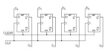
In addition to the above circuit, you will have two additional inputs. One (CLK) is shown above and represents the clock. When the clock and the other input (called ENABLE) are both set high (i.e. set to 1), then all four D flip flops shown in the diagram will load their D input values. If either the clock (CLK) or the ENABLE input are set low (i.e. set to 0), then the state of the D flip flop will be unchanged.
Do D2 D GET D . e CUR lo CUR CIR CA CLEAR CLK gol 02
Step by Step Solution
There are 3 Steps involved in it

Get step-by-step solutions from verified subject matter experts