PLEASE DO NOT COPY PASTE FROM CHEGG/OTHERWISE I'LL REPORT YOU OR GIVE OU A DISLIKE
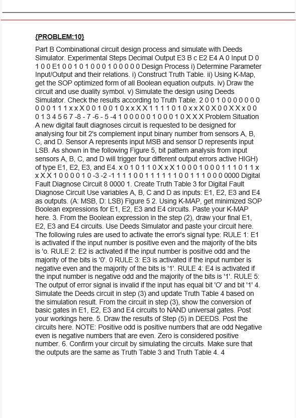
{PROBLEM:10} Part B Combinational circuit design process and simulate with Deeds Simulator. Experimental Steps Decimal Output E3 B C E2 E4 A 0 Input DO 100 E100101000100000 Design Process i) Determine Parameter Input/Output and their relations. i) Construct Truth Table. ii) Using K-Map, get the SOP optimized form of all Boolean equation outputs. iv) Draw the circuit and use duality symbol. v) Simulate the design using Deeds Simulator. Check the results according to Truth Table. 20010000000 000111xxX0010010XXXX1111010xxXOXOOXXX00 0134 5 6 7-8-7-6-5-4100000100010XXX Problem Situation A new digital fault diagnoses circuit is requested to be designed for analysing four bit 2's complement input binary number from sensors A, B, C, and D. Sensor A represents input MSB and sensor D represents input LSB. As shown in the following Figure 5, bit pattern analysis from input sensors A, B, C, and D will trigger four different output errors active HIGH) of type E1, E2, E3, and E4. X010110XXX 10001000111011x XXX1000010-3-2-11110011111100111000 0000 Digital Fault Diagnose Circuit 8 0000 1. Create Truth Table 3 for Digital Fault Diagnose Circuit Use variables A, B, C and D as inputs: E1, E2, E3 and E4 as outputs. (A: MSB, D: LSB) Figure 5 2. Using K-MAP, get minimized SOP Boolean expressions for E1, E2, E3 and E4 circuits. Paste your K-MAP here. 3. From the Boolean expression in the step (2), draw your final E1, E2, E3 and E4 circuits. Use Deeds Simulator and paste your circuit here. The following rules are used to activate the error's signal type: RULE 1: E1 is activated if the input number is positive even and the majority of the bits is 'O. RULE 2: E2 is activated if the input number is positive odd and the majority of the bits is 'O'. O RULE 3: E3 is activated if the input number is negative even and the majority of the bits is '1'. RULE 4: E4 is activated if the input number is negative odd and the majority of the bits is '1'. RULE 5: The output of error signal is invalid if the input has equal bit 'O' and bit '1' 4. Simulate the Deeds circuit in step (3) and update Truth Table 4 based on the simulation result. From the circuit in step (3), show the conversion of basic gates in E1, E2, E3 and E4 circuits to NAND universal gates. Post your workings here. 5. Draw the results of Step (5) in DEEDS. Post the circuits here. NOTE: Positive odd is positive numbers that are odd Negative even is negative numbers that are even. Zero is considered positive number. 6. Confirm your circuit by simulating the circuits. Make sure that the outputs are the same as Truth Table 3 and Truth Table 4.4 {PROBLEM:10} Part B Combinational circuit design process and simulate with Deeds Simulator. Experimental Steps Decimal Output E3 B C E2 E4 A 0 Input DO 100 E100101000100000 Design Process i) Determine Parameter Input/Output and their relations. i) Construct Truth Table. ii) Using K-Map, get the SOP optimized form of all Boolean equation outputs. iv) Draw the circuit and use duality symbol. v) Simulate the design using Deeds Simulator. Check the results according to Truth Table. 20010000000 000111xxX0010010XXXX1111010xxXOXOOXXX00 0134 5 6 7-8-7-6-5-4100000100010XXX Problem Situation A new digital fault diagnoses circuit is requested to be designed for analysing four bit 2's complement input binary number from sensors A, B, C, and D. Sensor A represents input MSB and sensor D represents input LSB. As shown in the following Figure 5, bit pattern analysis from input sensors A, B, C, and D will trigger four different output errors active HIGH) of type E1, E2, E3, and E4. X010110XXX 10001000111011x XXX1000010-3-2-11110011111100111000 0000 Digital Fault Diagnose Circuit 8 0000 1. Create Truth Table 3 for Digital Fault Diagnose Circuit Use variables A, B, C and D as inputs: E1, E2, E3 and E4 as outputs. (A: MSB, D: LSB) Figure 5 2. Using K-MAP, get minimized SOP Boolean expressions for E1, E2, E3 and E4 circuits. Paste your K-MAP here. 3. From the Boolean expression in the step (2), draw your final E1, E2, E3 and E4 circuits. Use Deeds Simulator and paste your circuit here. The following rules are used to activate the error's signal type: RULE 1: E1 is activated if the input number is positive even and the majority of the bits is 'O. RULE 2: E2 is activated if the input number is positive odd and the majority of the bits is 'O'. O RULE 3: E3 is activated if the input number is negative even and the majority of the bits is '1'. RULE 4: E4 is activated if the input number is negative odd and the majority of the bits is '1'. RULE 5: The output of error signal is invalid if the input has equal bit 'O' and bit '1' 4. Simulate the Deeds circuit in step (3) and update Truth Table 4 based on the simulation result. From the circuit in step (3), show the conversion of basic gates in E1, E2, E3 and E4 circuits to NAND universal gates. Post your workings here. 5. Draw the results of Step (5) in DEEDS. Post the circuits here. NOTE: Positive odd is positive numbers that are odd Negative even is negative numbers that are even. Zero is considered positive number. 6. Confirm your circuit by simulating the circuits. Make sure that the outputs are the same as Truth Table 3 and Truth Table 4.4


