

Question
Please help fix my code (I am using keil with texas instruments tiva launchpad c series tm4c123gxl) This is the assignment This is my code
Please help fix my code (I am using keil with texas instruments tiva launchpad c series tm4c123gxl)
This is the assignment
This is my code
; The programn tests gpio_a for input/output
; Setup
;
;
;
GPIO_PORTA_DATA_R EQU 0x400043FC
GPIO_PORTA_DIR_R EQU 0x40004400
GPIO_PORTA_AFSEL_R EQU 0x40004420
GPIO_PORTA_PUR_R EQU 0x40004510
GPIO_PORTA_DEN_R EQU 0x4000451C
GPIO_PORTA_LOCK_R EQU 0x40004520
GPIO_PORTA_CR_R EQU 0x40004524
GPIO_PORTA_AMSEL_R EQU 0x40004528
GPIO_PORTA_PCTL_R EQU 0x4000452C
GPIO_LOCK_KEY EQU 0x4C4F434B ; Unlocks the GPIO_CR register
....
....
SYSCTL_RCGC2_R EQU 0x400FE108
SYSCTL_RCGC2_GPIOA EQU 0x00000001 ; port A Clock Gating Control
;delay
ONESECOND EQU 5333333
AREA |.text|, CODE, READONLY, ALIGN=2
THUMB
EXPORT Start
Start
BL PortA_Init ; initialize input and output pins of
Port A
loop
LDR R0, =FIFTHSEC ; R0 = FIFTHSEC (delay 0.2 second)
BL delay ; delay at least (3*R0) cycles
BL PortA_Input ; read all of the switches on Port A
CMP R0, #0x01 ; R0 == 0x01?
BEQ sw1pressed
....
....
B loop
;
;
PortA_Init
LDR R1, =SYSCTL_RCGC2_R ; 1) activate clock for Port A
LDR R0, [R1]
ORR R0, R0, #0x01 ; set bit 1 to turn on clock
STR R0, [R1]
NOP
NOP ; allow time for clock to finish
LDR R1, =GPIO_PORTA_LOCK_R ; 2) unlock the lock register
LDR R0, =0x4C4F434B ; unlock GPIO Port A Commit Register
STR R0, [R1]
LDR R1, =GPIO_PORTA_CR_R ; enable commit for Port F
MOV R0, #0xFF ; 1 means allow access
STR R0, [R1]
LDR R1, =GPIO_PORTA_AMSEL_R ; 3) disable analog functionality
MOV R0, #0 ; 0 means analog is off
STR R0, [R1]
LDR R1, =GPIO_PORTA_PCTL_R ; 4) configure as GPIO
MOV R0, #0x00000000 ; 0 means configure Port A as GPIO
STR R0, [R1]
LDR R1, =GPIO_PORTA_DIR_R ; 5) set direction register
MOV R0,#0xE0 ; PA5-PA7 FOR OUTPUT and PA2 FOR input
STR R0, [R1]
LDR R1, =GPIO_PORTA_AFSEL_R ; 6) regular port function
MOV R0, #0 ; 0 means disable alternate function
STR R0, [R1]
LDR R1, =GPIO_PORTA_PUR_R ; pull-up resistors for PF4,PF0
MOV R0, #0x11 ; enable weak pull-up on PF0 and PF4
STR R0, [R1]
LDR R1, =GPIO_PORTA_DEN_R ; 7) enable Port F digital port
MOV R0, #0xFF ; 1 means enable digital I/O
STR R0, [R1]
BX LR
;
;GPIO_PORTE_BASE EQU 0X40024000
;GPIO_PORTF_BASE EQU 0X40025000
;GPIO_DATA_R EQU 0x3FC
;GPIO_DIR_R EQU 0x400
;GPIO_AFSEL_R EQU 0x420
;GPIO_PUR_R EQU 0x510
;GPIO_DEN_R EQU 0x51C
;GPIO_LOCK_R EQU 0x520
;GPIO_CR_R EQU 0x524
;GPIO_AMSEL_R EQU 0x528
;GPIO_PCTL_R EQU 0x52C
;GPIO_LOCK_KEY EQU 0x4C4F434B ; Unlocks the GPIO_CR register
; PA2: input switch
; PA5:LED Green
; PA6: LED Yellow
; PA7: LED Red
RED EQU 0x10
BLUE EQU 0x20
GREEN EQU 0x40
SW1 EQU 0x02 ; on the left side of the Launchpad board
;SW2 EQU 0x01 ; on the right side of the Launchpad board
SYSCTL_RCGC2_R EQU 0x400FE108
SYSCTL_RCGC2_GPIOA EQU 0x00000001 ; port A Clock Gating Control
AREA |.text|, CODE, READONLY, ALIGN=2
THUMB
EXPORT Start
Start
;Set initial value to the counter. Turn on LEDs
;STEP 4 Is the button (PA2) pressed? If not, wait.
;Increment the counter. Turn on LEDs
;Wait (Delay) for 1 second. (Use a function call, BL)
;Branch to Step 4)
bl init_port_a
bl clear
bl button
bl count
bl delay
loop bl led_on
;read the switch
count adds r1, r11
bx lr
delay ldr r0, =ONESECOND
b_delay_loop sub ro, #1
cmp r0, #0
bne b_delay_loop
bx lr
clear ldr r2, [GPIO_PORTA_DATA_R]
ldr r1, #0xe0
mvns r1, [r1]
and r2, r1 ; r2 = new destination register
str GPIO_PORTA_DATA_R, [r2]
ldr r11, #0
bx lr
button ;ldr r3, =GPIO_PORTA_BASE
ldr r0, [GPIO_PORTA_DATA_R]
and r0, r0, #0x04
cmp r0, #0x04
beq loop
; bl led_off
; nop
b button
; b loop
;
led_on ldr r3, =GPIO_PORTE_BASE
mov r0,#0x0ff
str r0, [r3, #GPIO_DATA_R]
bx lr
;
led_off ldr r3, =GPIO_PORTE_BASE
mov r0,#0x000
str r0, [r3, #GPIO_DATA_R]
bx lr
;
;
;init_port_e
; ldr r3, =SYSCTL_RCGC2_R ;turn on clock on port-e
; ldr r0, [r3]
; orr r0, r0, #0x020
; orr r0, r0, #0x010
; str r0, [r3]
; nop
; nop
; ldr r3, =GPIO_PORTE_BASE
; ldr r0, =GPIO_LOCK_KEY ;unlock the lock register
; str r0, [r3, #GPIO_LOCK_R]
; mov r0, #0x00f7 ;set all pins but pin-3 as output
; str r0, [r3, #GPIO_DIR_R]
; mov r0, #0xff ;set up pull-up registers
; str r0, [r3, #GPIO_PUR_R]
; mov r0, #0xff ;set up digital enable
; str r0, [r3, #GPIO_DEN_R]
; mov r0, #0xff ;set control register
; str r0, [r3, #GPIO_CR_R]
; bx lr
;
ALIGN ; make sure the end of this section is aligned
END ; end of file
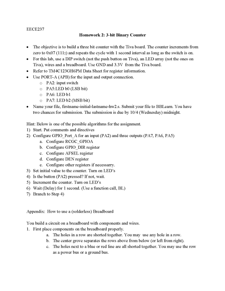
EECE237 Homework 2: 3-bit Binary Counter . The objective is to build a three bit counter with the Tiva board. The counter increments from zero to 0x07 (1112) and repeats the cycle with 1 second interval as long as the switch is on. For this lab, use a DIP switch (not the push button on Tiva), an LED array (not the ones on Tiva), wires and a breadboard. Use GND and 3.3V from the Tiva board . Refer to TM4C123GH6PM Data Sheet for register information . Use PORT-A (APB) for the input and output connection o PA2: input switch o PA5:LED b0 (LSB bit) o PA6: LED bl PA7: LED b2 (MSB bit) Name your file, firstname-initial-lastname-hw2.s. Submit your file to BBLearm. You have two chances for submission. The submission is due by 10/4 (Wednesday) midnight. Hint: Below is one of the possible algorithms for the assignment. 1) Start. Put comments and directives 2) Configure GPIO_Port A for an input (PA2) and three outputs (PA7, PA6, PA5) a. Configure RCGC GPIOA b. Configure GPIO DIR register c. Configure AFSEL register d. Configure DEN register e. Configure other registers if necessarry 3) Set initial value to the counter. Turn on LEDs 4) Is the button (PA2) pressed? If not, wait. 5) Increment the counter. Turn on LEDs 6) Wait (Delay) for 1 second. (Use a function call, BL) 7) Branch to Step 4) Appendix: How to use a (solderless) Breadboard You build a circuit on a breadboard with components and wires 1. First place components on the breadboard properly. a. b. c The holes in a row are shorted together. You may use any hole in a row The center grove separates the rows above from below (or left from right). The holes next to a blue or red line are all shorted together. You may use the row as a power bus or a ground bus EECE237 Homework 2: 3-bit Binary Counter . The objective is to build a three bit counter with the Tiva board. The counter increments from zero to 0x07 (1112) and repeats the cycle with 1 second interval as long as the switch is on. For this lab, use a DIP switch (not the push button on Tiva), an LED array (not the ones on Tiva), wires and a breadboard. Use GND and 3.3V from the Tiva board . Refer to TM4C123GH6PM Data Sheet for register information . Use PORT-A (APB) for the input and output connection o PA2: input switch o PA5:LED b0 (LSB bit) o PA6: LED bl PA7: LED b2 (MSB bit) Name your file, firstname-initial-lastname-hw2.s. Submit your file to BBLearm. You have two chances for submission. The submission is due by 10/4 (Wednesday) midnight. Hint: Below is one of the possible algorithms for the assignment. 1) Start. Put comments and directives 2) Configure GPIO_Port A for an input (PA2) and three outputs (PA7, PA6, PA5) a. Configure RCGC GPIOA b. Configure GPIO DIR register c. Configure AFSEL register d. Configure DEN register e. Configure other registers if necessarry 3) Set initial value to the counter. Turn on LEDs 4) Is the button (PA2) pressed? If not, wait. 5) Increment the counter. Turn on LEDs 6) Wait (Delay) for 1 second. (Use a function call, BL) 7) Branch to Step 4) Appendix: How to use a (solderless) Breadboard You build a circuit on a breadboard with components and wires 1. First place components on the breadboard properly. a. b. c The holes in a row are shorted together. You may use any hole in a row The center grove separates the rows above from below (or left from right). The holes next to a blue or red line are all shorted together. You may use the row as a power bus or a ground bus
Step by Step Solution
There are 3 Steps involved in it
Step: 1

Get Instant Access to Expert-Tailored Solutions
See step-by-step solutions with expert insights and AI powered tools for academic success
Step: 2

Step: 3
Ace Your Homework with AI
Get the answers you need in no time with our AI-driven, step-by-step assistance
Get Started
The Ultimate Apache Flink Introduction Streamlined Data Mastering Apache Flink For Real Time Processing
Authors: Big Data Landscape
1st Edition
B0CNN5YBX5, 979-8868164415