

Answered step by step
Verified Expert Solution
Question
1 Approved Answer
please Solve Step1: Write the truth table for the 7-segment display decoder. Step2: Derive a Boolean Expression from the truth table for each of the

please Solve Step1: Write the truth table for the 7-segment display decoder.
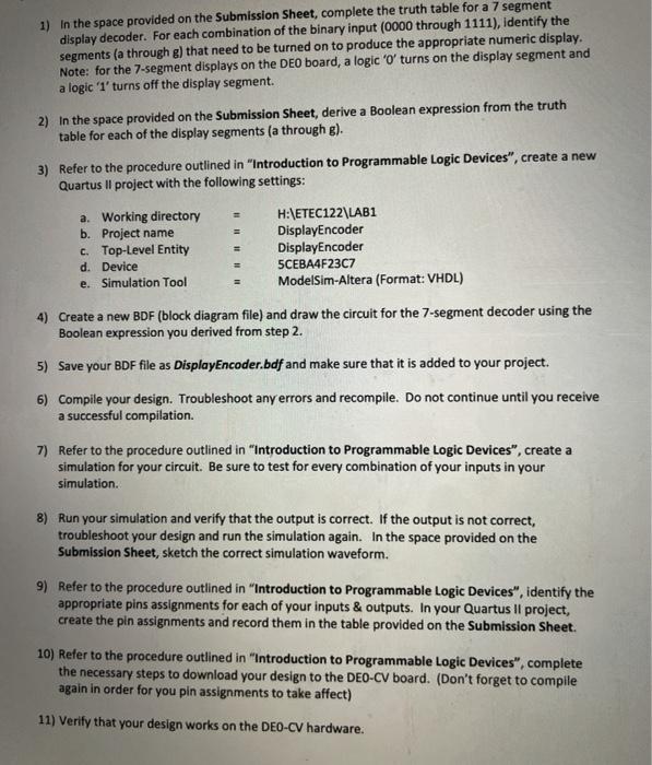
1) In the space provided on the Submission Sheet, complete the truth table for a 7 segment display decoder. For each combination of the binary input (0000 through 1111), identify the segments (a through g) that need to be turned on to produce the appropriate numeric display. Note: for the 7-segment displays on the DEO board, a logic 'o' turns on the display segment and a logic 'l' turns off the display segment. 2) In the space provided on the Submission Sheet, derive a Boolean expression from the truth table for each of the display segments (a through g). 3) Refer to the procedure outlined in "Introduction to Programmable Logic Devices", create a new Quartus Il project with the following settings: = a. Working directory b. Project name c. Top-Level Entity d. Device e. Simulation Tool = H:\ETEC122\LAB1 DisplayEncoder DisplayEncoder 5CEBA4F2307 ModelSim-Altera (Format: VHDL) 4) Create a new BDF (block diagram file) and draw the circuit for the 7-segment decoder using the Boolean expression you derived from step 2. 5) Save your BDF file as DisplayEncoder.bdf and make sure that it is added to your project. 6) Compile your design. Troubleshoot any errors and recompile. Do not continue until you receive a successful compilation. 7) Refer to the procedure outlined in "Introduction to Programmable Logic Devices", create a simulation for your circuit. Be sure to test for every combination of your inputs in your simulation. 8) Run your simulation and verify that the output is correct. If the output is not correct, troubleshoot your design and run the simulation again. In the space provided on the Submission Sheet, sketch the correct simulation waveform. 9) Refer to the procedure outlined in "Introduction to Programmable Logic Devices", identify the appropriate pins assignments for each of your inputs & outputs. In your Quartus Il project, create the pin assignments and record them in the table provided on the Submission Sheet. 10) Refer to the procedure outlined in "Introduction to Programmable Logic Devices", complete the necessary steps to download your design to the DEO-CV board. (Don't forget to compile again in order for you pin assignments to take affect) 11) Verify that your design works on the DEO-CV hardware. 12) Take all necessary steps to extend your design from 4 bits (one hex digit) to 8 bits (two hex digits). 13) Program your revised design onto the DEO-CV board and demonstrate proper functionality to your instructor. Have instructor sign the Submission Sheet for 8-bit (two hex digit) display functionality Step2: Derive a Boolean Expression from the truth table for each of the display segments (a through g)
Step8: Sketch the correct simulation waveform in the space below:
Step9: Pin assignments( Input/Output name,pin assignment, Location on DE0-CV Board)
Step by Step Solution
There are 3 Steps involved in it
Step: 1

Get Instant Access to Expert-Tailored Solutions
See step-by-step solutions with expert insights and AI powered tools for academic success
Step: 2

Step: 3
Ace Your Homework with AI
Get the answers you need in no time with our AI-driven, step-by-step assistance
Get Started
Big Data Concepts, Theories, And Applications
Authors: Shui Yu, Song Guo
1st Edition
3319277634, 9783319277639