

Question: Problems: 6.35(e,f) 368 Chapter 6 Registers and Counters Problems 369 PROBLEMS S1 So Register Operation No change Complement the four outputs Clear register to 0
Problems: 6.35(e,f)
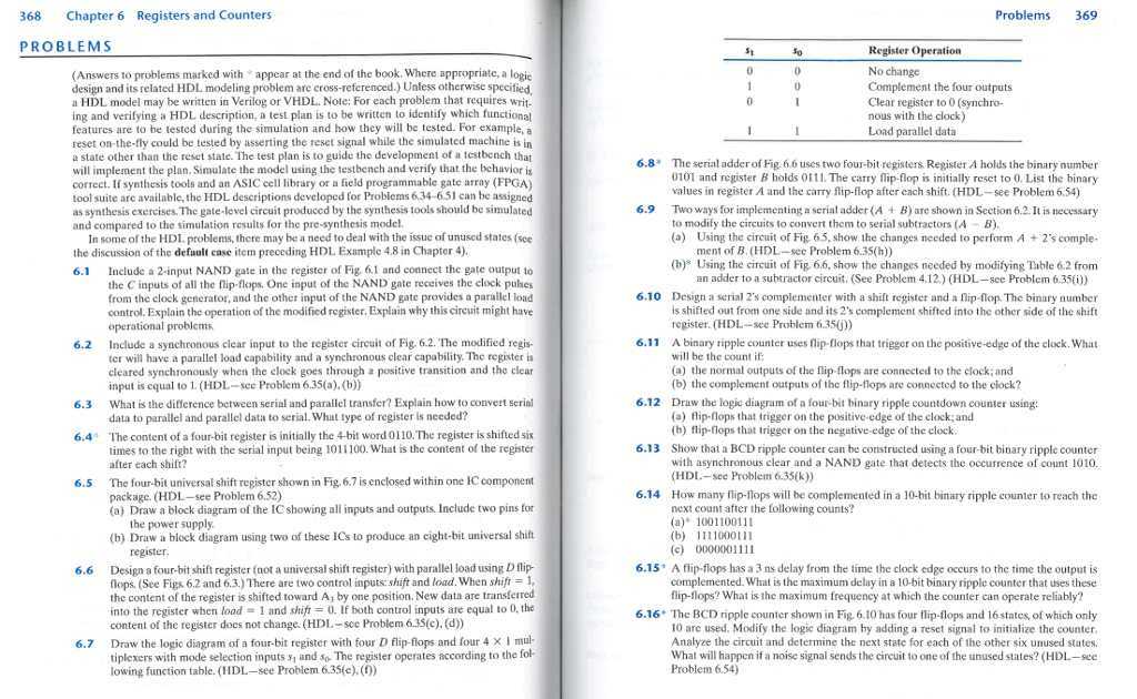
368 Chapter 6 Registers and Counters Problems 369 PROBLEMS S1 So Register Operation No change Complement the four outputs Clear register to 0 (synchro- nous with the clock) Load parallel data (Answers to problems marked with appcar at the end of the book. Where appropriate, a logic design and its related HDL modeling problem are cross-referenced.) Unless otherwisc specified, a HDL model may be written in Verilog or VHDL. Note: For each problem that requires writ ing and verifying a HDL description, a test plan is to be written to identify which functional features are to be tested during the simulation and how they will be tested. For example,a reset on-the-fly could be tested by asserting the reset signal while the simulated machine is in a state other than the reset state. The test plan is to guide the development of a testbench that will implement the plan. Simulate the model using the testbench and verify that the behavior is correct. If synthesis tools and an ASIC cell library or a field programmable gate array (FPGA) tool suite are available, the HDL descriptions developed for Problems 6.34-6.51 can be assigned as synthesis exercises.The gate-level circuit produced by the synthesis tools should be simulated 6.8 The serial adder of Fig.6.6 uses two four-bit registers. Register A holds the binary number 0101 and register B holds 0111. The carry flip-flop is initially reset to O. List the binary values in register A and the carry flip-flop after each shift. (HDL-see Problem 6.54) Two ways for implementing a serial adder (A B) are shown in Section 6.2. It is necessary to modify the circuits to convert them to serial subtractors (A B) a) Using the circuit of Fig 6.5, show the changes needed to perform A + 2's comple- 6.9 and compared to the simulation results for the pre-synthesis model. In some of the HDI. problems, there may be a need to deal with the issue of unused states (see the discussion of the default case item preccding HDL Example 4.8 in Chapter 4) ment of B. (HDL-see Problem 6.35(h)) (b) Using the circuit of Fig. 6.6, show the changes needed by modifying Table 6.2 from 6.1 Include a 2-input NAND gate in the register of Fig. 6.1 and connect the gate output to the C inputs of all the flip-flops. One input of the NAND gate receives the clock pulses from the clock generator, and the other input of the NAND gate provides a parallel load control. Explain the operation of the modified register. Explain why this circuit might have an adder to a subtractor circuit. (See Problem 4.12) (HDL-sce Problem 6.35(0)) 6.10 Design a serial 2's complementer with a shift register and a flip-flop. The binary number is shifted out from one side and its 2's complement shifted into the other side of the shift register. (HDL-see Problem 6.356)) operational problems 6.11 A binary ripple counter uses flip-flops that trigger on the positive-edge of the clock. What Include a synchronous clear input to the register circuit of Fig. 6.2. The modified regis- ter will have a parallel load capability and a synchronous clear capability. The register is cleared synchronously when the clock goes through a positive transition and the clear 6.2 will be the count if (a) the normal outputs of the flip-flops are connected to the clock; and (b) the complement outputs of the flip-flops are connected to the clock? Draw the logic diagram of a four-bit binary ripple countdown counter using: (a) flip-flops that trigger on the positive-edge of the clock: and (b) flip-flops that trigger on the negative-edge of the clock Show that a BCD ripple counter can be constructed using a four-bit binary ripple counter with asynchronous clear and a NAND gate that detects the occurrence of count 1010. (HDL-see Problem 6.35(k)) How many flip-flops will be complemented in a 10-bit binary ripple counter to reach the next count after the following counts? (a)1001100111 (b) 1111000111 (e) 0000001111 input is equal to 1. (HDL-see Problem 6.35(a).(b) 6.3 What is the difference between serial and parallel transfer? Explain how to convert serial 6.12 data to parallel and parallel data to serial. What type of register is needed? The content of a four-bit register is initially the 4-bit word 0110.The register is shifted six times to the right with the serial input being 1011100. What is the content of the register 6.4 6.13 after each shift? The four-bit universal shift register shown in Fig.6.7 is enclosed within one IC component (a) Draw a block diagram of the IC showing all inputs and outputs. Include two pins for (b) Draw a block diagram using two of these ICs to produce an cight-bit universal shift 6.5 package. (HDL-see Problem 6.52) 6.14 the power supply register Design a four-bit shift register (not a universal shift register) with parallel load using D flip- flops. (See Figs. 6.2 and 6.3.) There are two control inputs: shift and load. When shift , the content of the register is shifted toward A by one position. New data are transferred into the register when load = 1 and shift = O. If both control inputs are equal to 0, the 6.6 6.15 A flip-flops has a 3 ns delay from the time the clock edge occurs to the time the output is complemented. What is the maximum delay in a 10-bit binary ripple counter that uses these flip-flops? What is the maximum frequency at which the counter can operate reliably? 6.16 The BCD ripple counter shown in Fig.6.10 has four flip-flops and 16 states, of which only content of the register does not change. (HDL-see Problem 6.35(c), (d)) Draw the logic diagram of a four-bit register with four D flip-flops and four 4 l mul- iplexers with mode selection inputs s1 and so The register operates according to the fol- 10 are used. Modify the logic diagram by adding a reset signal to initialize the counter Analyze the circuit and determine the next state for each of the other six unused states. What will happen if a noise signal sends the circuit to one of the unused states? (HDL-see Problem 654) 6.7 lowing function table. (HDL-see Problem 6.35(e). (f)
Step by Step Solution
There are 3 Steps involved in it

Get step-by-step solutions from verified subject matter experts