

Question: Project Assignment 2018 A Simple Arithmetic Logic Unit Page 1 af2 Arithmetic and Logic Units (or ALUs) are found at the core of microprocessors, where
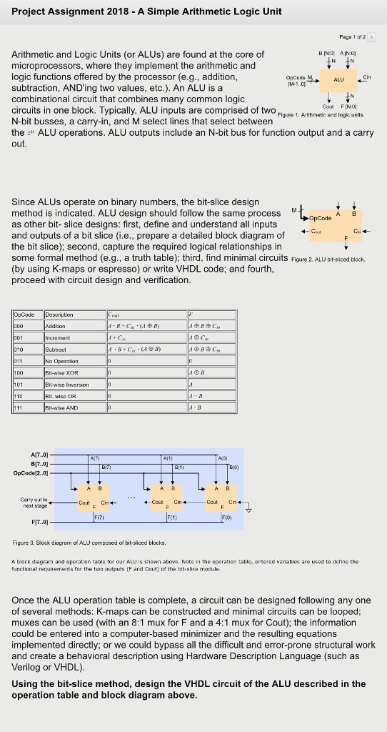
Project Assignment 2018 A Simple Arithmetic Logic Unit Page 1 af2 Arithmetic and Logic Units (or ALUs) are found at the core of microprocessors, where they implement the arithmetic and logic functions offered by the processor (e.g., addition subtraction, AND'ing two values, etc.). An ALU is a combinational circuit that combines many common logic circuits in one block. Typically, ALU inputs are comprised of two N-bit busses, a carry-in, and M select lines that select between the 2" ALU operations. ALU outputs include an N-bit bus for function output and a carry out. OpCode ALU Con FINO Figure 1, Artthmetic end logic units Since ALUs operate on binary numbers, the bit-slice design method is indicated. ALU design should follow the same process M as other bit- slice designs: first, define and understand all inputs and outputs of a bit slice (i.e., prepare a detailed block diagram of the bit slice); second, capture the required logical relationships in some formal method (e.g., a truth table); third, find minimal circuits Figure 2. ALU bit-siced block. (by using K-maps or espresso) or write VHDL code; and fourth proceed with circuit design and verification +OpCode A B (AB) ubtrac Bit-wise XOR 101 it-wise Irversion Bit-wisa AND A B A7.0] B[7.0) OpCodel2.0] AI1 E(o) A 0 A B A B Cary out ko next stag0 4 -Cout Cin Cout Cn F[7.0) Figure 3. Block diagram of ALU composed of bit-siced blucks. A block diagram and operation table for our ALU is shown above. Note in the operation table, entered variables are used to define the functional recuirements for the two outputs (F and Cout) of the bit-slice module Once the ALU operation table is complete, a circuit can be designed following any one of several methods: K-maps can be constructed and minimal circuits can be looped muxes can be used (with an 8:1 mux for F and a 4:1 mux for Cout); the information could be entered into a computer-based minimizer and the resulting equations implemented directly; or we could bypass all the difficult and error-prone structural work and create a behavioral description using Hardware Description Language (such as Verilog or VHDL) Using the bit-slice method, design the VHDL circuit of the ALU described in the operation table and block diagram above Project Assignment 2018 A Simple Arithmetic Logic Unit Page 1 af2 Arithmetic and Logic Units (or ALUs) are found at the core of microprocessors, where they implement the arithmetic and logic functions offered by the processor (e.g., addition subtraction, AND'ing two values, etc.). An ALU is a combinational circuit that combines many common logic circuits in one block. Typically, ALU inputs are comprised of two N-bit busses, a carry-in, and M select lines that select between the 2" ALU operations. ALU outputs include an N-bit bus for function output and a carry out. OpCode ALU Con FINO Figure 1, Artthmetic end logic units Since ALUs operate on binary numbers, the bit-slice design method is indicated. ALU design should follow the same process M as other bit- slice designs: first, define and understand all inputs and outputs of a bit slice (i.e., prepare a detailed block diagram of the bit slice); second, capture the required logical relationships in some formal method (e.g., a truth table); third, find minimal circuits Figure 2. ALU bit-siced block. (by using K-maps or espresso) or write VHDL code; and fourth proceed with circuit design and verification +OpCode A B (AB) ubtrac Bit-wise XOR 101 it-wise Irversion Bit-wisa AND A B A7.0] B[7.0) OpCodel2.0] AI1 E(o) A 0 A B A B Cary out ko next stag0 4 -Cout Cin Cout Cn F[7.0) Figure 3. Block diagram of ALU composed of bit-siced blucks. A block diagram and operation table for our ALU is shown above. Note in the operation table, entered variables are used to define the functional recuirements for the two outputs (F and Cout) of the bit-slice module Once the ALU operation table is complete, a circuit can be designed following any one of several methods: K-maps can be constructed and minimal circuits can be looped muxes can be used (with an 8:1 mux for F and a 4:1 mux for Cout); the information could be entered into a computer-based minimizer and the resulting equations implemented directly; or we could bypass all the difficult and error-prone structural work and create a behavioral description using Hardware Description Language (such as Verilog or VHDL) Using the bit-slice method, design the VHDL circuit of the ALU described in the operation table and block diagram above
Step by Step Solution
There are 3 Steps involved in it

Get step-by-step solutions from verified subject matter experts