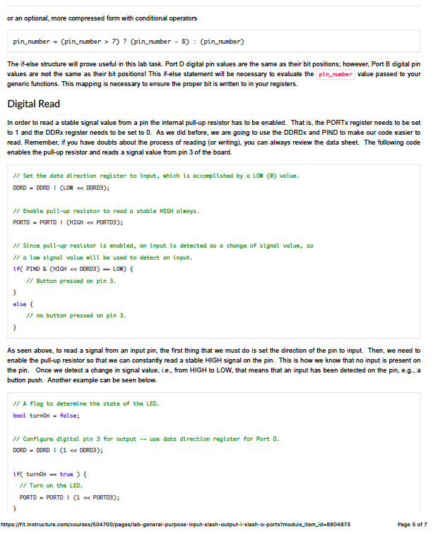
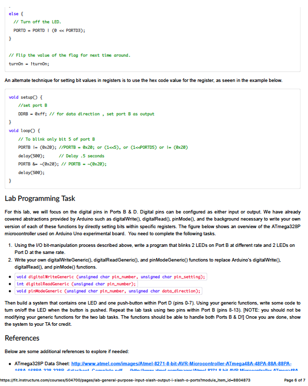
Provide details and explanation as a comment, please...


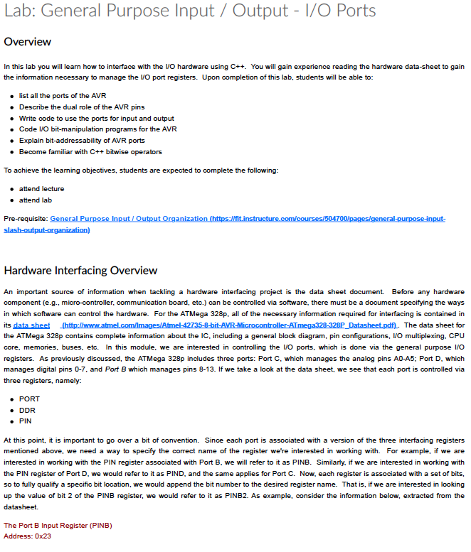
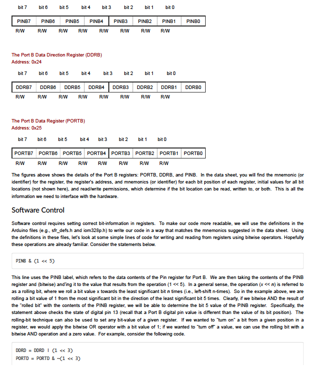
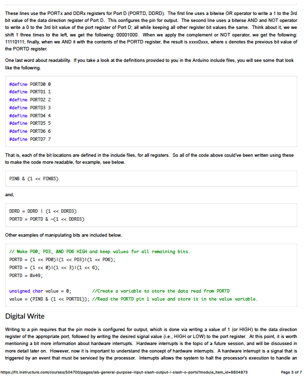
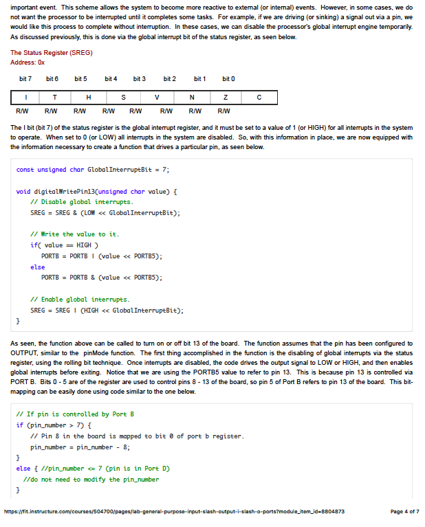
Lab: General Purpose Input/ Output - I/O Ports Overview In this lab you will learn how to interface with the VO hardware using C++. You will gain experience reading the hardware data-sheet to gain the information necessary to manage the WO port registers. U Upon of this lab, students will be able to: list all the ports of the AVR Describe the dual role of the AVR Write code to use the ports for input and output Code I/O bit-manipulation programs for the AVR Explain bit-addressability of AVR ports . Become familiar with C++ bitwise operators To achieve the learning objectives, students are expected to complete the following attend lecture attend lab Hardware Interfacing Overview An important source of information when tackling a hardware interfacing project is the data sheet document. Before any hardware component (e.g., micro-controller, communication board, etc.) can be controlled via software, there must be a document specifying the ways in which software can control the hardware. For the ATMega 328p, all of the necessary information required for interfacing is contained in its dlata sheet the ATMega 328p contains complete information about the IC, including a general block diagram, pin configurations, VO multiplexing, CPU core, memories, buses, etc. In this module, we are interested in controlling the LO ports, which is done via the general purpose VO registers. As previously discussed, the ATMega 328p includes three ports: Port C, which manages the analog pins A0-A5; Port D, which manages digital pins 0-7, and Port B which manages pins 8-13. If we take a look at the data sheet, we see that each port is controlled via three registers, namely The data sheet for PORT DDR e PIN At this point, it is important to go over a bit of convention. Since each port is associated with a version of the three interfacing registers mentioned above, we need a way to specify the correct name of the register we're interested in working with. For example, if we are interested in working with the PIN register associated with Port B, we will refer to it as PINB. Similarly, if we are interested in working with the PIN register of Port D, we would refer to it as PIND, and the same applies for Port C. Now, each register is associated with a set of bits, so to fully qualify a specific bit location, we would append the bit number to the desired register name. That is, if we are interested in looking up the value of bit 2 of the PINB register, we would refer to it as PINB2. As example, consider the information below, extracted from the datasheet. The Port B Input Register (PINB) Address: 0x23 Lab: General Purpose Input/ Output - I/O Ports Overview In this lab you will learn how to interface with the VO hardware using C++. You will gain experience reading the hardware data-sheet to gain the information necessary to manage the WO port registers. U Upon of this lab, students will be able to: list all the ports of the AVR Describe the dual role of the AVR Write code to use the ports for input and output Code I/O bit-manipulation programs for the AVR Explain bit-addressability of AVR ports . Become familiar with C++ bitwise operators To achieve the learning objectives, students are expected to complete the following attend lecture attend lab Hardware Interfacing Overview An important source of information when tackling a hardware interfacing project is the data sheet document. Before any hardware component (e.g., micro-controller, communication board, etc.) can be controlled via software, there must be a document specifying the ways in which software can control the hardware. For the ATMega 328p, all of the necessary information required for interfacing is contained in its dlata sheet the ATMega 328p contains complete information about the IC, including a general block diagram, pin configurations, VO multiplexing, CPU core, memories, buses, etc. In this module, we are interested in controlling the LO ports, which is done via the general purpose VO registers. As previously discussed, the ATMega 328p includes three ports: Port C, which manages the analog pins A0-A5; Port D, which manages digital pins 0-7, and Port B which manages pins 8-13. If we take a look at the data sheet, we see that each port is controlled via three registers, namely The data sheet for PORT DDR e PIN At this point, it is important to go over a bit of convention. Since each port is associated with a version of the three interfacing registers mentioned above, we need a way to specify the correct name of the register we're interested in working with. For example, if we are interested in working with the PIN register associated with Port B, we will refer to it as PINB. Similarly, if we are interested in working with the PIN register of Port D, we would refer to it as PIND, and the same applies for Port C. Now, each register is associated with a set of bits, so to fully qualify a specific bit location, we would append the bit number to the desired register name. That is, if we are interested in looking up the value of bit 2 of the PINB register, we would refer to it as PINB2. As example, consider the information below, extracted from the datasheet. The Port B Input Register (PINB) Address: 0x23
