

Answered step by step
Verified Expert Solution
Question
1 Approved Answer
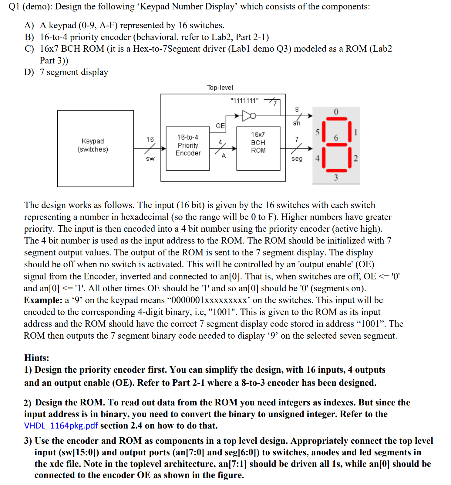
Q 1 ( demo ) : Design the following 'Keypad Number Display' which consists of the components: A ) A keypad ( 0 - 9
Qdemo: Design the following 'Keypad Number Display' which consists of the components:
A A keypad AF represented by switches.
Bto priority encoder behavioral refer to Lab Part
C BCH ROM it is a HextoSegment driver Lab demo Q modeled as a ROM Lab
Part
D segment display
The design works as follows. The input bit is given by the switches with each switch
representing a number in hexadecimal so the range will be to F Higher numbers have greater
priority. The input is then encoded into a bit number using the priority encoder active high
The bit number is used as the input address to the ROM. The ROM should be initialized with
segment output values. The output of the ROM is sent to the segment display. The display
should be off when no switch is activated. This will be controlled by an 'output enable' OE
signal from the Encoder, inverted and connected to an That is when switches are off,
and an All other times OE should be and so an should be segments on
Example: a on the keypad means on the switches. This input will be
encoded to the corresponding digit binary, ie This is given to the ROM as its input
address and the ROM should have the correct segment display code stored in address The
ROM then outputs the segment binary code needed to display on the selected seven segment.
Hints:
Design the priority encoder first. You can simplify the design, with inputs, outputs
and an output enable OE Refer to Part where a to encoder has been designed.
Design the ROM. To read out data from the ROM you need integers as indexes. But since the
input address is in binary, you need to convert the binary to unsigned integer. Refer to the
VHDLpkgpdf section on how to do that.
Use the encoder and ROM as components in a top level design. Appropriately connect the top level
input sw: and output ports an: and seg: to switches, anodes and led segments in
the xdc file. Note in the toplevel architecture, an: should be driven all while an should be
connected to the encoder as shown in the figure.
Step by Step Solution
There are 3 Steps involved in it
Step: 1

Get Instant Access to Expert-Tailored Solutions
See step-by-step solutions with expert insights and AI powered tools for academic success
Step: 2

Step: 3
Ace Your Homework with AI
Get the answers you need in no time with our AI-driven, step-by-step assistance
Get Started
Big Data Systems A 360-degree Approach
Authors: Jawwad ShamsiMuhammad Khojaye
1st Edition
0429531575, 9780429531576