Answered step by step
Verified Expert Solution
Question
1 Approved Answer
Q3. An amorphous nanolayer of two different electronic-grade compounds were deposited onto some sapphire substrates by a process called DC magnetron sputtering. The deposited thin
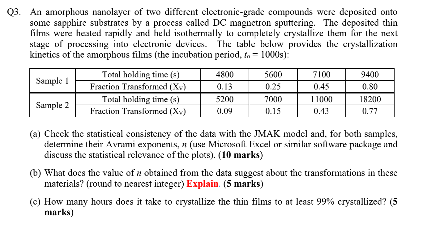
Q3. An amorphous nanolayer of two different electronic-grade compounds were deposited onto some sapphire substrates by a process called DC magnetron sputtering. The deposited thin films were heated rapidly and held isothermally to completely crystallize them for the next stage of processing into electronic devices. The table below provides the crystallization kinetics of the amorphous films (the incubation period, to = 1000s): 9400 Sample 1 0.80 Total holding time (s) Fraction Transformed (Xy) Total holding time (s) Fraction Transformed (Xy) 4800 0.13 5200 0.09 5600 0.25 7000 0.15 7100 0.45 11000 0.43 Sample 2 18200 0.77 (a) Check the statistical consistency of the data with the JMAK model and, for both samples, determine their Avrami exponents, n (use Microsoft Excel or similar software package and discuss the statistical relevance of the plots). (10 marks) (b) What does the value of n obtained from the data suggest about the transformations in these materials? (round to nearest integer) Explain. (5 marks) (c) How many hours does it take to crystallize the thin films to at least 99% crystallized
Step by Step Solution
There are 3 Steps involved in it
Step: 1
Get Instant Access to Expert-Tailored Solutions
See step-by-step solutions with expert insights and AI powered tools for academic success
Step: 2
Step: 3
Ace Your Homework with AI
Get the answers you need in no time with our AI-driven, step-by-step assistance
Get Started