Answered step by step
Verified Expert Solution
Question
1 Approved Answer
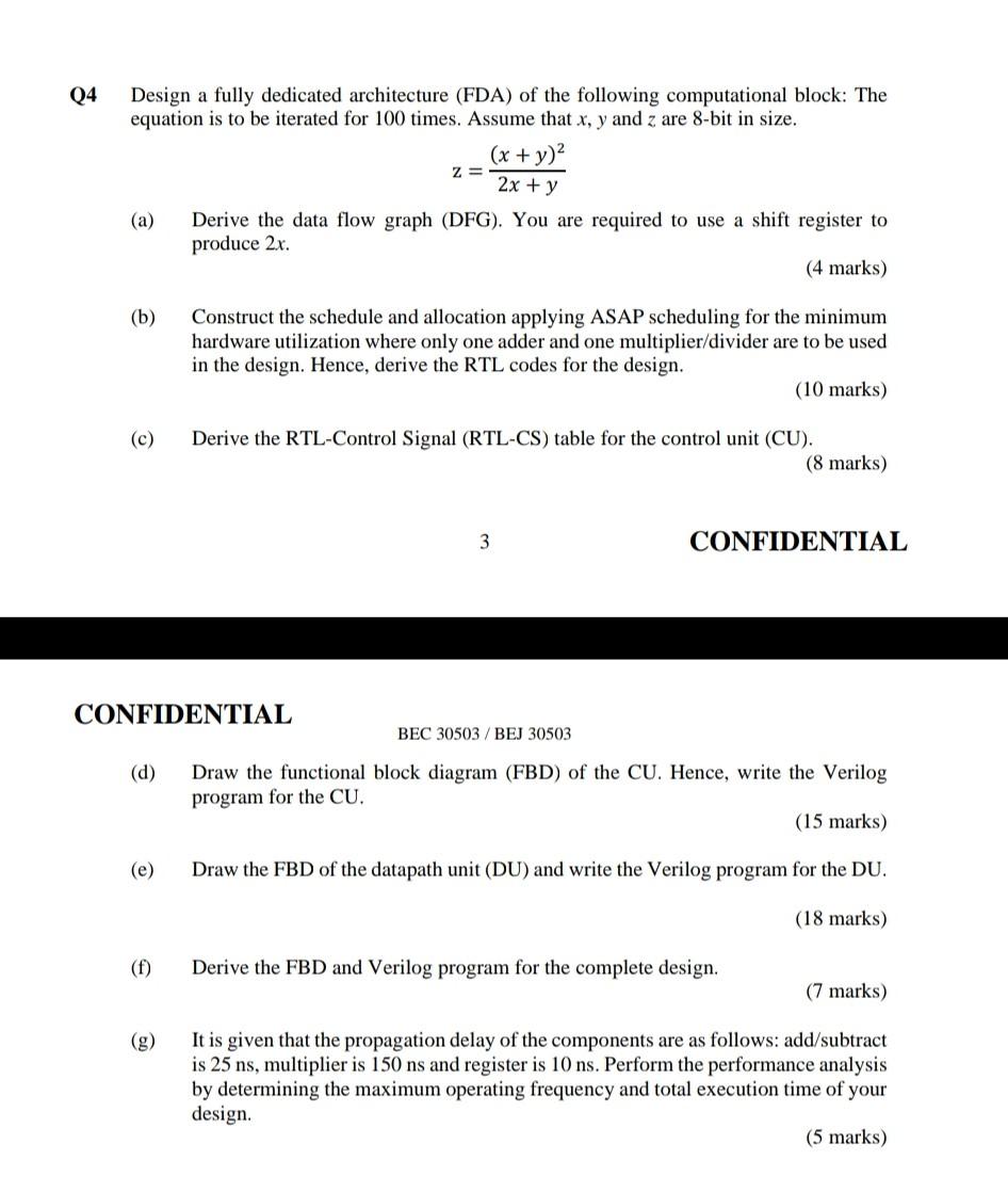
Q4 Z= Design a fully dedicated architecture (FDA) of the following computational block: The equation is to be iterated for 100 times. Assume that x,

Q4 Z= Design a fully dedicated architecture (FDA) of the following computational block: The equation is to be iterated for 100 times. Assume that x, y and z are 8-bit in size. (x + y)2 2x + y (a) Derive the data flow graph (DFG). You are required to use a shift register to produce 2x. (4 marks) (b) Construct the schedule and allocation applying ASAP scheduling for the minimum hardware utilization where only one adder and one multiplier/divider are to be used in the design. Hence, derive the RTL codes for the design. (10 marks) (c) Derive the RTL-Control Signal (RTL-CS) table for the control unit (CU). (8 marks) 3 CONFIDENTIAL CONFIDENTIAL BEC 30503 /BEJ 30503 (d) Draw the functional block diagram (FBD) of the CU. Hence, write the Verilog program for the CU. (15 marks) (e) Draw the FBD of the datapath unit (DU) and write the Verilog program for the DU. (18 marks) (f) Derive the FBD and Verilog program for the complete design. (7 marks) It is given that the propagation delay of the components are as follows: add/subtract is 25 ns, multiplier is 150 ns and register is 10 ns. Perform the performance analysis by determining the maximum operating frequency and total execution time of your design. (5 marks) Q4 Z= Design a fully dedicated architecture (FDA) of the following computational block: The equation is to be iterated for 100 times. Assume that x, y and z are 8-bit in size. (x + y)2 2x + y (a) Derive the data flow graph (DFG). You are required to use a shift register to produce 2x. (4 marks) (b) Construct the schedule and allocation applying ASAP scheduling for the minimum hardware utilization where only one adder and one multiplier/divider are to be used in the design. Hence, derive the RTL codes for the design. (10 marks) (c) Derive the RTL-Control Signal (RTL-CS) table for the control unit (CU). (8 marks) 3 CONFIDENTIAL CONFIDENTIAL BEC 30503 /BEJ 30503 (d) Draw the functional block diagram (FBD) of the CU. Hence, write the Verilog program for the CU. (15 marks) (e) Draw the FBD of the datapath unit (DU) and write the Verilog program for the DU. (18 marks) (f) Derive the FBD and Verilog program for the complete design. (7 marks) It is given that the propagation delay of the components are as follows: add/subtract is 25 ns, multiplier is 150 ns and register is 10 ns. Perform the performance analysis by determining the maximum operating frequency and total execution time of your design
Step by Step Solution
There are 3 Steps involved in it
Step: 1

Get Instant Access to Expert-Tailored Solutions
See step-by-step solutions with expert insights and AI powered tools for academic success
Step: 2

Step: 3

Ace Your Homework with AI
Get the answers you need in no time with our AI-driven, step-by-step assistance
Get Started


