Question
Q5/ Design an 1/0 port decoder that salect ponts : ( so, s2, s4,s6)H for out put data in lowbank ;( s1,s3, s5, s7), for

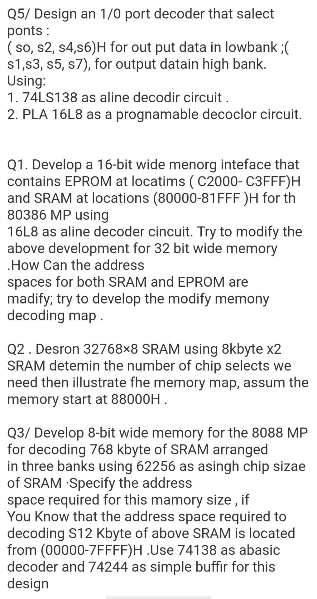
Q5/ Design an 1/0 port decoder that salect ponts : ( so, s2, s4,s6)H for out put data in lowbank ;( s1,s3, s5, s7), for output datain high bank. Using: 1.74LS138 as aline decodir circuit . 2. PLA 16L8 as a prognamable decoclor circuit. Q1. Develop a 16-bit wide menorg inteface that contains EPROM at locatims ( C2000- C3FFF)H and SRAM at locations (80000-81FFF )H for th 80386 MP using 16L8 as aline decoder cincuit. Try to modify the above development for 32 bit wide memory .How Can the address spaces for both SRAM and EPROM are madify; try to develop the modify memony decoding map .
Q2. Desron 32768x8 SRAM using 8kbyte x2 SRAM detemin the number of chip selects we need then illustrate fhe memory map, assum the memory start at 88000H.
Q3/ Develop 8-bit wide memory for the 8088 MP for decoding 768 kbyte of SRAM arranged in three banks using 62256 as asingh chip sizae of SRAM Specify the address space required for this mamory size , if You Know that the address space required to decoding S12 Kbyte of above SRAM is located from (00000-7FFFF)H.Use 74138 as abasic decoder and 74244 as simple buffir for this design
Q5/ Design an 1/0 port decoder that salect ponts : (so, s2, 54,56)H for out put data in lowbank ;( $1,53, 55, 57), for output datain high bank. Using: 1. 74LS138 as aline decodir circuit. 2. PLA 16L8 as a prognamable decoclor circuit. Q1. Develop a 16-bit wide menorg inteface that contains EPROM at locatims (C2000-C3FFF)H and SRAM at locations (80000-81FFF )H for th 80386 MP using 16L8 as aline decoder cincuit. Try to modify the above development for 32 bit wide memory .How Can the address spaces for both SRAM and EPROM are madify; try to develop the modify memony decoding map. Q2. Desron 32768x8 SRAM using 8kbyte x2 SRAM detemin the number of chip selects we need then illustrate fhe memory map, assum the memory start at 88000H. Q3/ Develop 8-bit wide memory for the 8088 MP for decoding 768 kbyte of SRAM arranged in three banks using 62256 as asingh chip sizae of SRAM Specify the address space required for this mamory size , if You know that the address space required to decoding S12 Kbyte of above SRAM is located from (00000-7FFFF)H .Use 74138 as abasic decoder and 74244 as simple buffor for this design Q5/ Design an 1/0 port decoder that salect ponts : (so, s2, 54,56)H for out put data in lowbank ;( $1,53, 55, 57), for output datain high bank. Using: 1. 74LS138 as aline decodir circuit. 2. PLA 16L8 as a prognamable decoclor circuit. Q1. Develop a 16-bit wide menorg inteface that contains EPROM at locatims (C2000-C3FFF)H and SRAM at locations (80000-81FFF )H for th 80386 MP using 16L8 as aline decoder cincuit. Try to modify the above development for 32 bit wide memory .How Can the address spaces for both SRAM and EPROM are madify; try to develop the modify memony decoding map. Q2. Desron 32768x8 SRAM using 8kbyte x2 SRAM detemin the number of chip selects we need then illustrate fhe memory map, assum the memory start at 88000H. Q3/ Develop 8-bit wide memory for the 8088 MP for decoding 768 kbyte of SRAM arranged in three banks using 62256 as asingh chip sizae of SRAM Specify the address space required for this mamory size , if You know that the address space required to decoding S12 Kbyte of above SRAM is located from (00000-7FFFF)H .Use 74138 as abasic decoder and 74244 as simple buffor for this designStep by Step Solution
There are 3 Steps involved in it
Step: 1

Get Instant Access to Expert-Tailored Solutions
See step-by-step solutions with expert insights and AI powered tools for academic success
Step: 2

Step: 3

Ace Your Homework with AI
Get the answers you need in no time with our AI-driven, step-by-step assistance
Get Started


