

Answered step by step
Verified Expert Solution
Question
1 Approved Answer
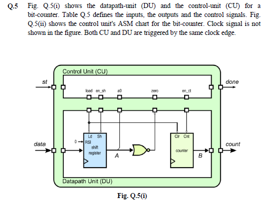
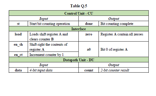
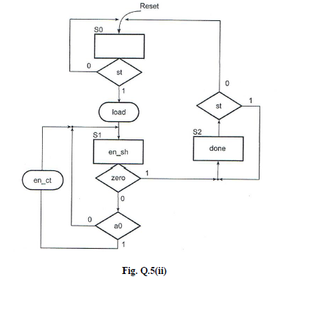
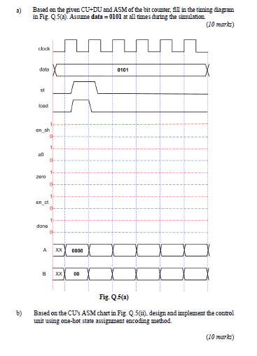
Q.5 Fig. 2.5(1) shows the datapath-unit (DU) and the control-unit (CU) for a bit-counter. Table Q.5 defines the inputs, the outputs and the control signals.
Step by Step Solution
There are 3 Steps involved in it
Step: 1

Get Instant Access to Expert-Tailored Solutions
See step-by-step solutions with expert insights and AI powered tools for academic success
Step: 2

Step: 3
Ace Your Homework with AI
Get the answers you need in no time with our AI-driven, step-by-step assistance
Get Started
Advanced MySQL 8 Discover The Full Potential Of MySQL And Ensure High Performance Of Your Database
Authors: Eric Vanier ,Birju Shah ,Tejaswi Malepati
1st Edition
1788834445, 978-1788834445