Answered step by step
Verified Expert Solution
Question
1 Approved Answer
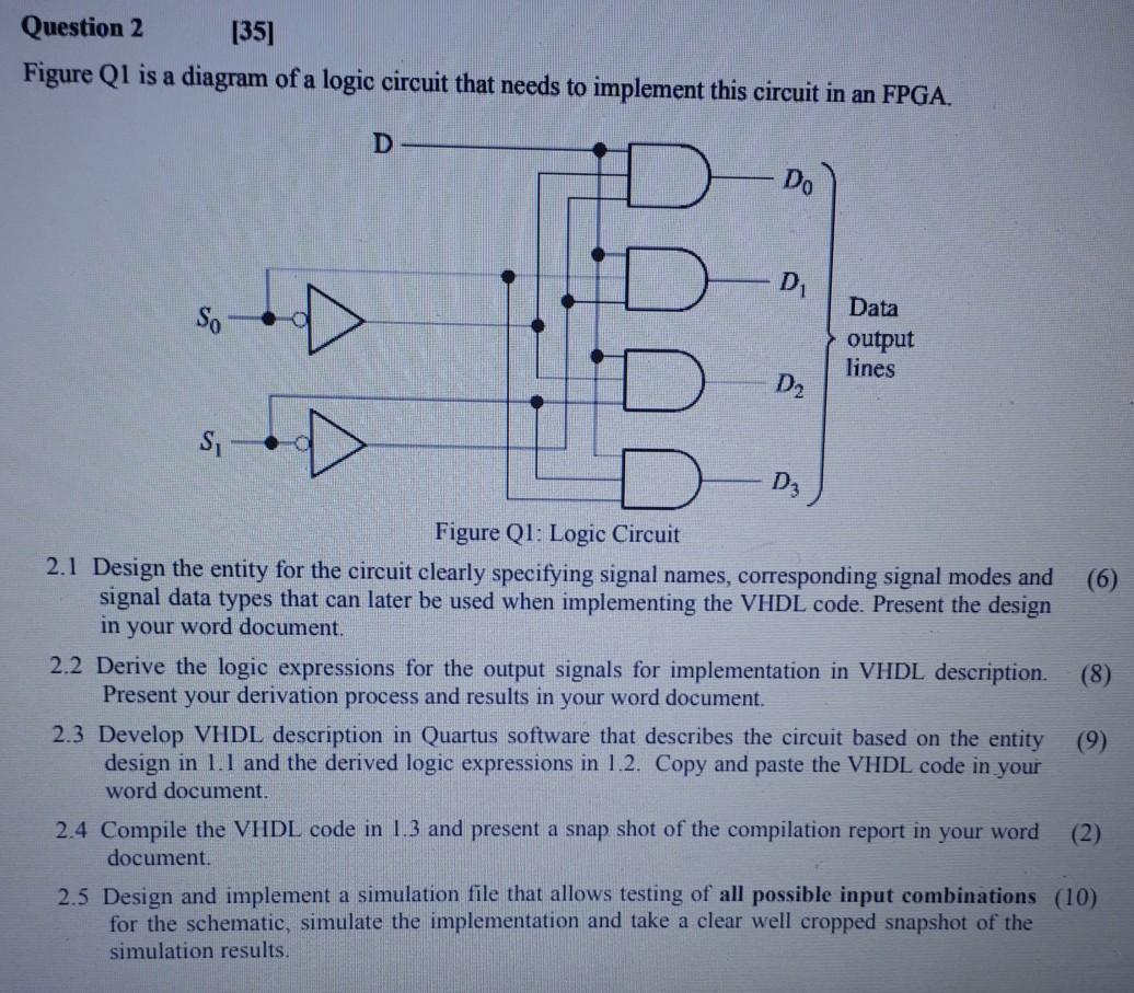
Question 2 [35] Figure Q1 is a diagram of a logic circuit that needs to implement this circuit in an FPGA. D Do D Data

Question 2 [35] Figure Q1 is a diagram of a logic circuit that needs to implement this circuit in an FPGA. D Do D Data So output lines B Si D Figure Q1: Logic Circuit 2.1 Design the entity for the circuit clearly specifying signal names, corresponding signal modes and (6) signal data types that can later be used when implementing the VHDL code. Present the design in your word document, 2.2 Derive the logic expressions for the output signals for implementation in VHDL description. (8) Present your derivation process and results in your word document, 2.3 Develop VHDL description in Quartus software that describes the circuit based on the entity (9) design in 1.1 and the derived logic expressions in 1.2. Copy and paste the VHDL code in your word document. 2.4 Compile the VHDL code in 1.3 and present a snap shot of the compilation report in your word (2) document. 2.5 Design and implement a simulation file that allows testing of all possible input combinations (10) for the schematic, simulate the implementation and take a clear well cropped snapshot of the simulation results. Question 2 [35] Figure Q1 is a diagram of a logic circuit that needs to implement this circuit in an FPGA. D Do D Data So output lines B Si D Figure Q1: Logic Circuit 2.1 Design the entity for the circuit clearly specifying signal names, corresponding signal modes and (6) signal data types that can later be used when implementing the VHDL code. Present the design in your word document, 2.2 Derive the logic expressions for the output signals for implementation in VHDL description. (8) Present your derivation process and results in your word document, 2.3 Develop VHDL description in Quartus software that describes the circuit based on the entity (9) design in 1.1 and the derived logic expressions in 1.2. Copy and paste the VHDL code in your word document. 2.4 Compile the VHDL code in 1.3 and present a snap shot of the compilation report in your word (2) document. 2.5 Design and implement a simulation file that allows testing of all possible input combinations (10) for the schematic, simulate the implementation and take a clear well cropped snapshot of the simulation results
Step by Step Solution
There are 3 Steps involved in it
Step: 1

Get Instant Access to Expert-Tailored Solutions
See step-by-step solutions with expert insights and AI powered tools for academic success
Step: 2

Step: 3

Ace Your Homework with AI
Get the answers you need in no time with our AI-driven, step-by-step assistance
Get Started


