Answered step by step
Verified Expert Solution
Question
1 Approved Answer
Qurstion: Write the function by Boolean Algebra and truth table. Digital Logic ( CS201) Lab 9: Hexadecimal digit counter using Nexys 3 FPGA Board Objective:
Qurstion: Write the function by Boolean Algebra and truth table. 
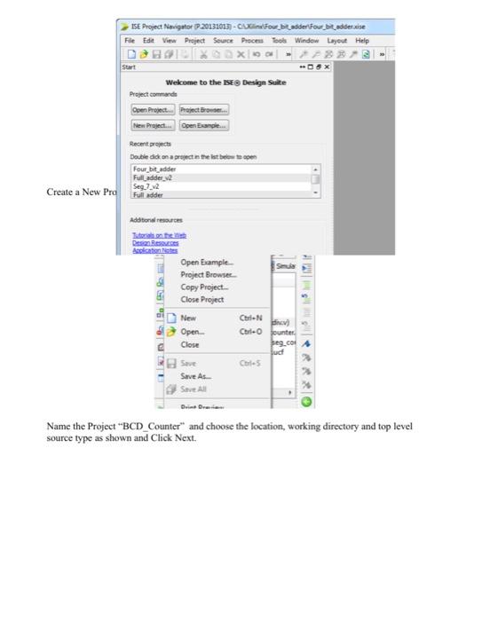
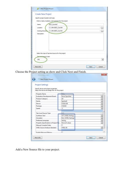
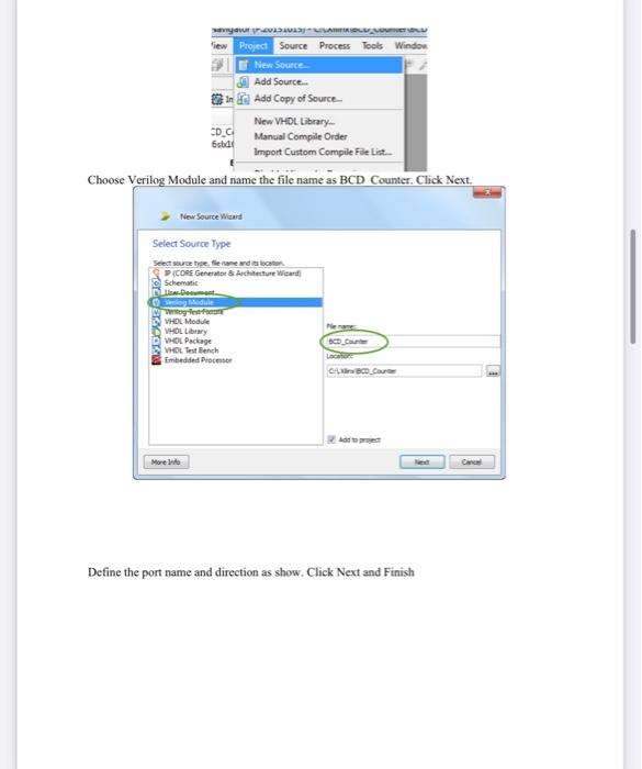
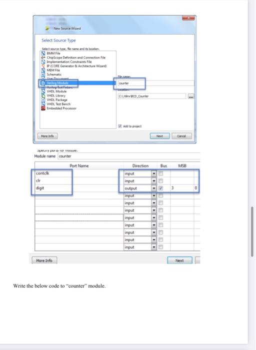
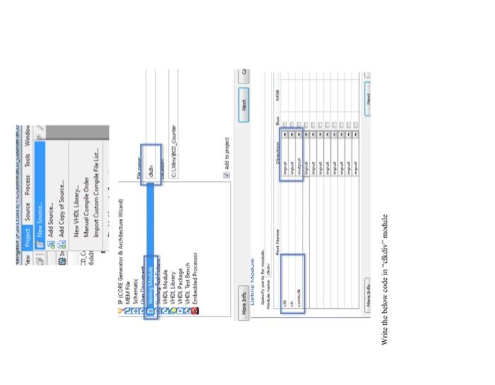
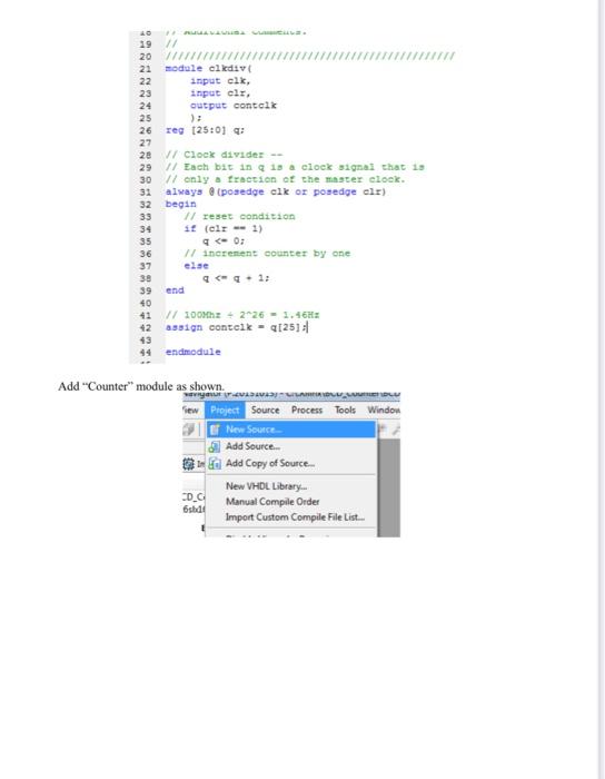
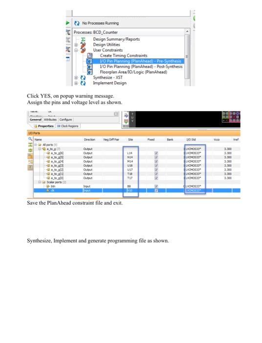
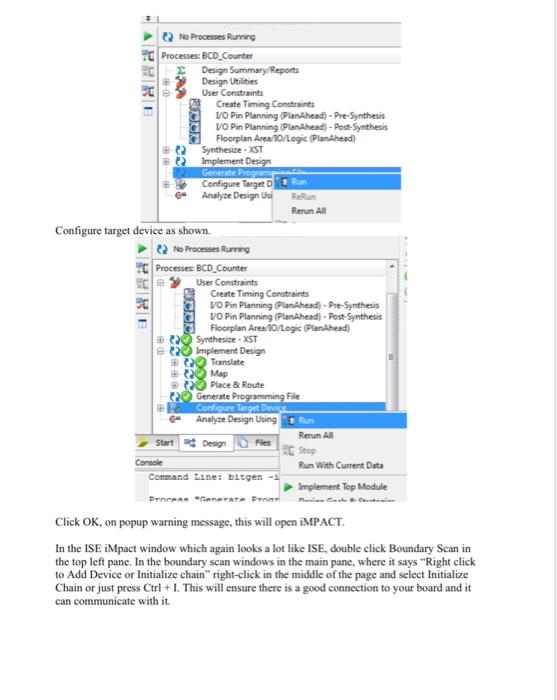
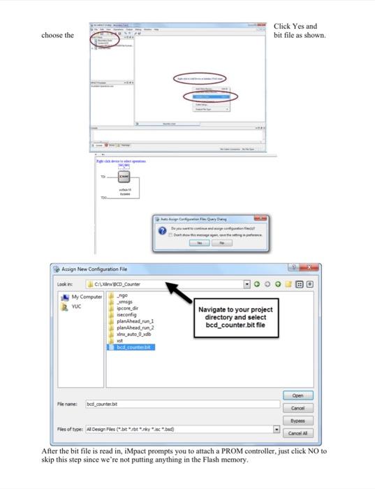
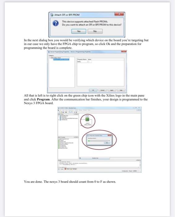
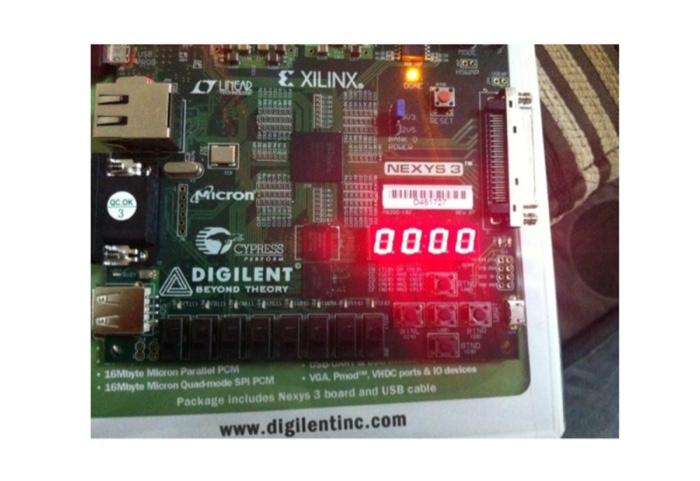

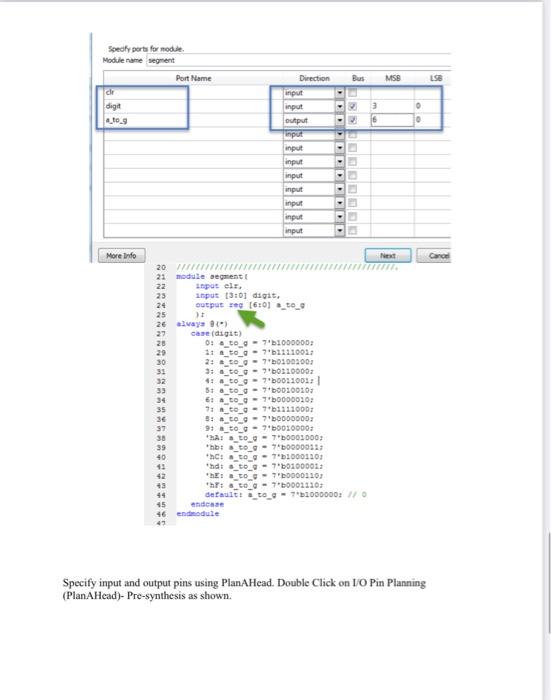
Digital Logic ( CS201) Lab 9: Hexadecimal digit counter using Nexys 3 FPGA Board Objective: In this lab exercise students will be introduced to build a Hexadecimal counter using and Verilog hardware description language (Verilog HDL) and implement it in Nexys 3 FPGA board. The students will learn to develop a verilog code using multiple modules. Equipment Needed: - 1SE webpack software - Nexys 3 FPGA Board. Introduction : Verilog HDL is a language used to do describe circuits. It has many levels. The highest level allows the designer to describe a design by its behavior, using equations or using functional model. Hexadecimal digits can be displayed on seven-segment displays. A combination of uppercase and lowercase letters is used for AF; this is done to obtain a unique, unambiguous shape for each hexadecimal digit (otherwise, a capital D would look identical to an 0 and a capital B would look identical to an 8 ). Also the digit 6 must be displayed with the top bar lit to avoid ambiguity with the letter b. PART1: Procedure: Open the Xilinx ISE Design Suit 14.7. You can click on the ISE icon on the desktop, or search Start All Programs Xilinx ISE Design Suite 14.7 ISE Design Tools Project Navigator OR Double click on the desktop shortcut icon Welcome to the 15E 9 Design Sulte Project commands Recert propect Doulle did en a rupect in Bie lat beces te epen Four bit_adder Full adderav Seg.7_v2 Create a New Pro full adder Addbonal resources Wuterah on fickithe Deronfiesurcer Aaslcaben Neter Name the Project "BCD_Counter" and choose the location, working directory and top level source type as shown and Click Next. Nerin frept Wases Propect Sentings Add a New Source file to your project. Choose I Define the port name and direction as show. Click Next and Finish Write the below code to "counter" module. Write the below code in "clkdiv" module Add "Counter" module as shown. Click YES, on popup warning message. Assign the pins and voltage level as shown. Save the PlanAhead constraint file and exit. Synthesize, Implement and generate programming file as shown. Cd No Processes Rurring Configure target device as shown. Click OK, on popup warning message, this will open iMPACT. In the ISE iMpact window which again looks a lot like ISF, double click Boundary Scan in the top left pane. In the boundary scan windows in the main pane, where it says "Right click to Add Device or Initialize chain" right-click in the middle of the page and select Initialize Chain or just press Ctrl +1. This will ensure there is a good connection to your board and it can communicate with it. Click Yes and choose the bit file as shown. Assign New Configuration File Leok ins Cililirabel Counter ngo amigh ipcere,dir Navigate to your project directory and select plonAhead run_l bcd_counter.bit file siru_auto_0_yab ist Flenane: bod_counterbt After the bit file is read in, iMpact prompts you to attach a PROM controller, just click NO to skip this step since we're not putting anything in the Flash memory. (2. This sevict supports attached Flach FhoMr. De you wart to attach an SPI or BPI BECM to this device? In the next dialog box you would be verifying which device on the board you're targeting but in our case we only have the FPGA chip to program, so click Ok and the preparation for programming the board is complete. All that is left is to right click on the green chip icon with the Xilinx logo in the main pane and click. Program. After the communication bar finishes, your design is programmed to the Nexys 3 FPGA board. You are done. The nexys 3 board should count from 0 to F as shown. Cd No Processes Rurring Configure target device as shown. Click OK, on popup warning message, this will open iMPACT. In the ISE iMpact window which again looks a lot like ISF, double click Boundary Scan in the top left pane. In the boundary scan windows in the main pane, where it says "Right click to Add Device or Initialize chain" right-click in the middle of the page and select Initialize Chain or just press Ctrl +1. This will ensure there is a good connection to your board and it can communicate with it. Specify input and output pins using PlanAHead. Double Click on IO Pin Planning (PlanAHead)- Pre-synthesis as shown 


Step by Step Solution
There are 3 Steps involved in it
Step: 1

Get Instant Access to Expert-Tailored Solutions
See step-by-step solutions with expert insights and AI powered tools for academic success
Step: 2

Step: 3

Ace Your Homework with AI
Get the answers you need in no time with our AI-driven, step-by-step assistance
Get Started


