

Answered step by step
Verified Expert Solution
Question
1 Approved Answer
SHIFT REGISTER USING JK FLIP-FLOPS Objective(s): In this experiment, you will be able to use IK flip-flops to construct a shift register and test the
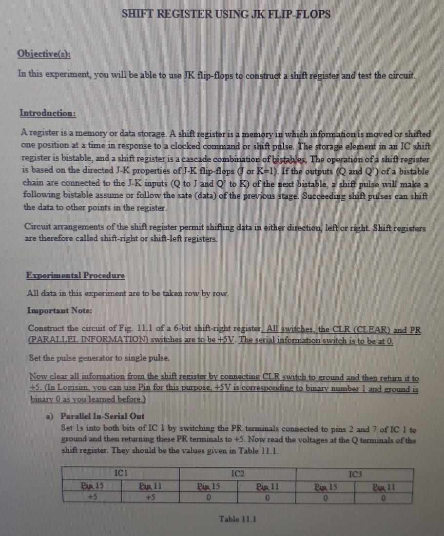
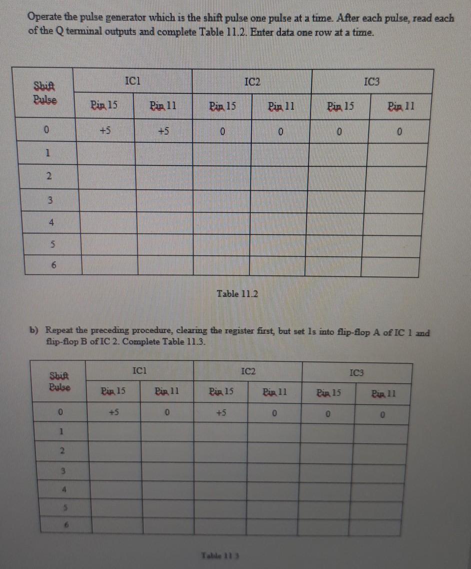
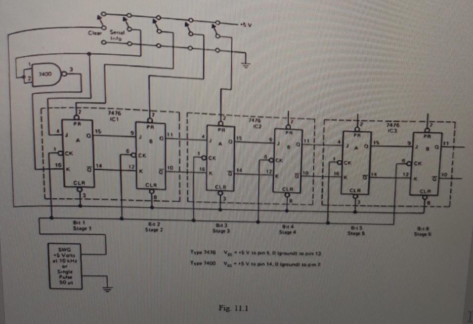
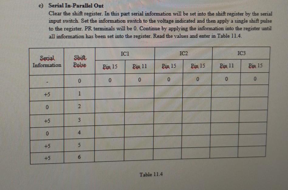
SHIFT REGISTER USING JK FLIP-FLOPS Objective(s): In this experiment, you will be able to use IK flip-flops to construct a shift register and test the circuit Introduction: A register is a memory or data storage. A shift register is a memory in which information is moved or shifted one position at a time in response to a clocked command or shift pulse. The storage element in an IC shift register is bistable, and a shift register is a cascade combination of bistables. The operation of a shift register is based on the directed J-K properties of J-K flip-flops or K=1). If the outputs (Q and Q") of a bistable chain are connected to the J-K inputs (Q to J and Q to K) of the next bistable, a shift pulse will make a following bistable assume or follow the sate (data) of the previous stage. Succeeding shift pulses can shift the data to other points in the register. Circuit arrangements of the shift register permit shifting data in either direction, left or night. Shift registers are therefore called shift-right or shift-left registers. Experimental Procedure All data in this experiment are to be taken row by row. Important Note: Construct the circuit of Fig. 11.1 of a 6-bit shift-right register. All switches, the CLR (CLEAR) and PR (PARALLEL INFORMATION switches are to be +5V. The serial information switch is to be at 0. Set the pulse generator to single pulse. Now clear all information from the shift register by connecting CLR switch to ground and then retum it to +5. (In Logisim, you can use Pin for this purpose +5V is corresponding to binary mumber 1 and ground is binary as you learned before.) a) Parallel In-Serial Out Set is into both bits of IC i by switching the PR terminals connected to pins 2 and 7 of IC 1 to ground and then returning these PR terminals to +5. Now read the voltages at the Q terminals of the shift register. They should be the values given in Table 11.1. ICI IC 2 IC3 Pun 15 Pin 11 +5 Pix 15 0 Pin 11 0 Pir 15 0 Pun 0 Table 11.1 Operate the pulse generator which is the shift pulse one pulse at a time. After each pulse, read each of the Q terminal outputs and complete Table 11.2. Enter data one row at a time. Ici IO IC3 Shit Pulse Pir 15 Pin 11 Pin 15 Pin 11 Pin 15 Pia, 11 0 +5 +5 0 0 0 0 1 3 4 5 6 Table 11.2 b) Repeat the preceding procedure, clearing the register first, but set ls into flip-flop A of IC 1 and flip-flop B of IC 2. Complete Table 11.3. ICI 102 IC3 Shifi Pulse Pix 15 Pin 11 Pia 15 Pin 11 Pir 15 Pin 11 0 +5 0 +5 0 0 0 1 2 3 4 5 6 Table 1 Info 7000 2476 IC1 PR M2 15 09 dick CW M 16 2 g 1 CLA CLR CL CIR 2 Stage S DO So a Sea SWG - VON 10 H TV 2430 Me M. TYMO 4.0 or 1 ? DOM Fig. 11.1 c) Serial In-Parallel Out Clear the shift register. In this part serial information will be set into the shift register by the serial input switch. Set the information switch to the voltage indicated and then apply a single shift pulse to the register. PR terminals will be 0. Continue by applying the information into the register until all information has been set into the register. Read the values and enter in Table 11.4. ICI IO2 IC3 Serial Information Shif Pulse Pia 15 Pin 11 Pir 15 Pin 15 Pin 11 Per 15 0 0 0 0 0 0 0 +5 1 0 2 +5 3 4 +5 5 +5 6 Table 11.4 SHIFT REGISTER USING JK FLIP-FLOPS Objective(s): In this experiment, you will be able to use IK flip-flops to construct a shift register and test the circuit Introduction: A register is a memory or data storage. A shift register is a memory in which information is moved or shifted one position at a time in response to a clocked command or shift pulse. The storage element in an IC shift register is bistable, and a shift register is a cascade combination of bistables. The operation of a shift register is based on the directed J-K properties of J-K flip-flops or K=1). If the outputs (Q and Q") of a bistable chain are connected to the J-K inputs (Q to J and Q to K) of the next bistable, a shift pulse will make a following bistable assume or follow the sate (data) of the previous stage. Succeeding shift pulses can shift the data to other points in the register. Circuit arrangements of the shift register permit shifting data in either direction, left or night. Shift registers are therefore called shift-right or shift-left registers. Experimental Procedure All data in this experiment are to be taken row by row. Important Note: Construct the circuit of Fig. 11.1 of a 6-bit shift-right register. All switches, the CLR (CLEAR) and PR (PARALLEL INFORMATION switches are to be +5V. The serial information switch is to be at 0. Set the pulse generator to single pulse. Now clear all information from the shift register by connecting CLR switch to ground and then retum it to +5. (In Logisim, you can use Pin for this purpose +5V is corresponding to binary mumber 1 and ground is binary as you learned before.) a) Parallel In-Serial Out Set is into both bits of IC i by switching the PR terminals connected to pins 2 and 7 of IC 1 to ground and then returning these PR terminals to +5. Now read the voltages at the Q terminals of the shift register. They should be the values given in Table 11.1. ICI IC 2 IC3 Pun 15 Pin 11 +5 Pix 15 0 Pin 11 0 Pir 15 0 Pun 0 Table 11.1 Operate the pulse generator which is the shift pulse one pulse at a time. After each pulse, read each of the Q terminal outputs and complete Table 11.2. Enter data one row at a time. Ici IO IC3 Shit Pulse Pir 15 Pin 11 Pin 15 Pin 11 Pin 15 Pia, 11 0 +5 +5 0 0 0 0 1 3 4 5 6 Table 11.2 b) Repeat the preceding procedure, clearing the register first, but set ls into flip-flop A of IC 1 and flip-flop B of IC 2. Complete Table 11.3. ICI 102 IC3 Shifi Pulse Pix 15 Pin 11 Pia 15 Pin 11 Pir 15 Pin 11 0 +5 0 +5 0 0 0 1 2 3 4 5 6 Table 1 Info 7000 2476 IC1 PR M2 15 09 dick CW M 16 2 g 1 CLA CLR CL CIR 2 Stage S DO So a Sea SWG - VON 10 H TV 2430 Me M. TYMO 4.0 or 1 ? DOM Fig. 11.1 c) Serial In-Parallel Out Clear the shift register. In this part serial information will be set into the shift register by the serial input switch. Set the information switch to the voltage indicated and then apply a single shift pulse to the register. PR terminals will be 0. Continue by applying the information into the register until all information has been set into the register. Read the values and enter in Table 11.4. ICI IO2 IC3 Serial Information Shif Pulse Pia 15 Pin 11 Pir 15 Pin 15 Pin 11 Per 15 0 0 0 0 0 0 0 +5 1 0 2 +5 3 4 +5 5 +5 6 Table 11.4
Step by Step Solution
There are 3 Steps involved in it
Step: 1

Get Instant Access to Expert-Tailored Solutions
See step-by-step solutions with expert insights and AI powered tools for academic success
Step: 2

Step: 3
Ace Your Homework with AI
Get the answers you need in no time with our AI-driven, step-by-step assistance
Get Started
Privacy In Statistical Databases International Conference Psd 2022 Paris France September 21 23 2022 Proceedings Lncs 13463
Authors: Josep Domingo-Ferrer ,Maryline Laurent
1st Edition
3031139445, 978-3031139444