

Question: Solve 1.a&b EXPERIMENT: SIMPLE DIGITAL DESIGN AND TTL Chips. References Introduction to Digital Design Using Digilent FPGA Boards: Appendix C - Basic Logic Gates. PRE-LAB
 Solve 1.a&b
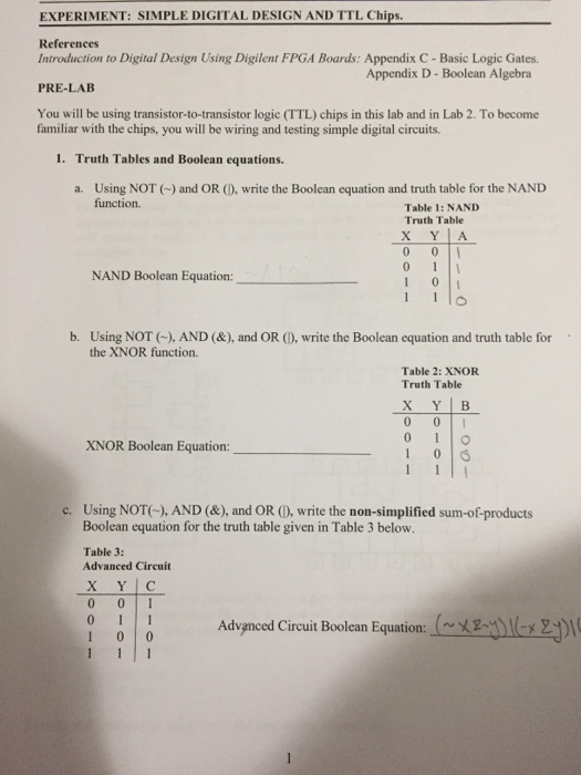
 EXPERIMENT: SIMPLE DIGITAL DESIGN AND TTL Chips. References Introduction to Digital Design Using Digilent FPGA Boards: Appendix C - Basic Logic Gates. PRE-LAB You will be using transistor-to-transistor logic (TTL) chips in this lab and in Lab 2. To become Appendix D- Boolean Algebra familiar with the chips, you will be wiring and testing simple digital circuits. 1. Truth Tables and Boolean equations. Using NOT and OR (1), write the Boolean equation and truth table for the NAND function. a. Table 1: NAND Truth Table NAND Boolean Equation: b. Using NOT ), AND (&), and OR (D. write the Boolean equation and truth table for the XNOR function. Table 2: XNOR Truth Table XNOR Boolean Equation:1 c. Using NOT), AND (&), and OR (D, write the non-simplified sum-of-products Boolean equation for the truth table given in Table 3 below Table 3: Advanced Circuit 0 Adygncod Cireuit Boolean Equatioe
Step by Step Solution
There are 3 Steps involved in it

Get step-by-step solutions from verified subject matter experts