Question
Some Example Code Given ALU from Lab 5 module ALU(A, B, reset, opcode,result ); input [8:0] A, B; input reset; input [2:0] opcode; output reg


Some Example Code Given

ALU from Lab 5
module ALU(A, B, reset, opcode,result );
input [8:0] A, B;
input reset;
input [2:0] opcode;
output reg [16:0]result;
always @(A or B or reset or opcode)
begin
if(reset == 1) begin
result
end
else begin
case(opcode)
7'b000 : result
7'b001 : result
7'b010 : result
7'b011 : result
7'b100 : result
7'b101 : result
7'b110 : result
7'b111 : result
endcase
end
end
endmodule
ALU Test Bench
module ALUTb();
reg [8:0] A, B;
reg [2:0] opcode;
reg reset;
reg [2:0]i;
wire [16:0] result;
ALU AUT0(A, B, reset, opcode,result);
initial
begin
reset = 1 ;
#10
reset = 0;
for (i=0;i
begin
opcode = i ;
A = 8'b11111111;
B = 8'b00000001;
#10;
end
end
endmodule
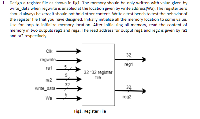
1. Design a register file as shown in fig1. The memory should be only written with value given by write_data when regwrite is enabled at the location given by write address(Wa). The register zero should always be zero; it should not hold other content. Write a test bench to test the behavior of the register file that you have designed. Initially initialize all the memory location to some value. Use for loop to initialize memory location. After initializing all memory, read the content of memory in two outputs reg1 and reg2. The read address for output reg1 and reg2 is given by ra1 and ra2 respectively. Clk regwrite ra1 ra2 32 reg1 32 32 register file 32 write_data 32 Wa reg2 Fig1. Register File 1. Design a register file as shown in fig1. The memory should be only written with value given by write_data when regwrite is enabled at the location given by write address(Wa). The register zero should always be zero; it should not hold other content. Write a test bench to test the behavior of the register file that you have designed. Initially initialize all the memory location to some value. Use for loop to initialize memory location. After initializing all memory, read the content of memory in two outputs reg1 and reg2. The read address for output reg1 and reg2 is given by ra1 and ra2 respectively. Clk regwrite ra1 ra2 32 reg1 32 32 register file 32 write_data 32 Wa reg2 Fig1. Register FileStep by Step Solution
There are 3 Steps involved in it
Step: 1

Get Instant Access to Expert-Tailored Solutions
See step-by-step solutions with expert insights and AI powered tools for academic success
Step: 2

Step: 3

Ace Your Homework with AI
Get the answers you need in no time with our AI-driven, step-by-step assistance
Get Started


