Answered step by step
Verified Expert Solution
Question
1 Approved Answer
SUB: DIGITAL DESGN Q: Controller's High-Level State Machine Diagram Thank you for your time and efforts, truly. If you took the trouble to understand one

SUB: DIGITAL DESGN
Q: Controller's High-Level State Machine Diagram
Thank you for your time and efforts, truly.
If you took the trouble to understand one to solve, there are also different questions on the same topic in my profile.
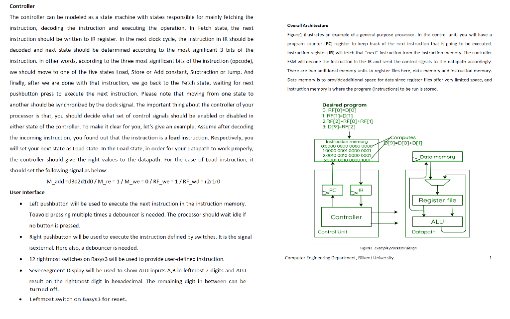
Controller Overall Architecture Figure1 illustrates an example of a general-purpose processor. In the control unit, you will have a program counter (PC) register to keep track of the next instruction that is going to be executed. Instruction register (IR) will fetch that "next" instruction from the instruction memory. The controller FSM will decode the Instruction in the IR and send the control signals to the datapath accordingly. There are two additional memory units to register files here, data memory and instruction memory Data memory is to provide additional space for data since register files offer very limited space, and instruction memory is where the program (instructions to be run is stored. The controller can be modeled as a state machine with states responsible for mainly fetching the instruction, decoding the instruction and executing the operation. In Fetch state, the next instruction should be written to IR register. In the next clock cycle, the instruction in IR should be decoded and next state should be determined according to the most significant 3 of the instruction. In other words, according to the three most significant bits of the instruction (opcode), we should move to one of the five states Load, Store or Add constant, Subtraction or Jump. And finally, after we are done with that instruction, we go back to the Fetch state, waiting for next pushbutton press to execute the next instruction. Please note that moving from one state to another should be synchronized by the clock signal. The important thing about the controller of your processor is that, you should decide what set of control signals should be enabled or disabled in either state of the controller. To make it clear for you, let's give an example. Assume after decoding the incoming instruction, you found out that the instruction is a load instruction. Respectively, you will set your next state as Load state. In the load state, in order for your datapath to work properly, the controller should give the right values to the datapath. For the case of Load instruction, it should set the following signal as below: M_add=d3d2d1do/M_re = 1 / M_we = 0 / RF_we = 1 / RF_wd = r2r110 User Interface Desired program O: RF0-Droi 1: RF01-01 2:RF[2]-RF[O]+RFC 3: D[9]-RF[2] . Computes Instruction 0 0000 0000 0000 0000 0193=D[0]+D[ 0]1 10000 0001 0000 0001 2:0010 0010 0000 0001 Data memory 300 TO COD.100 L PC IR Register file Left pushbutton will be used to execute the next instruction in the instruction memory. Toavoid pressing multiple times a debouncer is needed. The processor should wait idle if Controller ALU no button is pressed. Control Unit Datapath Figurel. Example processar design . 1 Computer Engineering Department, Bilkent University Right pushbutton will be used to execute the instruction defined by switches. It is the signal isexternal. Here also, a debouncer is needed. 12 rightmost switches on Basys3 will be used to provide user-defined instruction, SevenSegment Display will be used to show ALU inputs A, B in leftmost 2 digits and ALU result on the rightmost digit in hexadecimal. The remaining digit in between can be turned off. Leftmost switch on Basys3 for reset. Controller Overall Architecture Figure1 illustrates an example of a general-purpose processor. In the control unit, you will have a program counter (PC) register to keep track of the next instruction that is going to be executed. Instruction register (IR) will fetch that "next" instruction from the instruction memory. The controller FSM will decode the Instruction in the IR and send the control signals to the datapath accordingly. There are two additional memory units to register files here, data memory and instruction memory Data memory is to provide additional space for data since register files offer very limited space, and instruction memory is where the program (instructions to be run is stored. The controller can be modeled as a state machine with states responsible for mainly fetching the instruction, decoding the instruction and executing the operation. In Fetch state, the next instruction should be written to IR register. In the next clock cycle, the instruction in IR should be decoded and next state should be determined according to the most significant 3 of the instruction. In other words, according to the three most significant bits of the instruction (opcode), we should move to one of the five states Load, Store or Add constant, Subtraction or Jump. And finally, after we are done with that instruction, we go back to the Fetch state, waiting for next pushbutton press to execute the next instruction. Please note that moving from one state to another should be synchronized by the clock signal. The important thing about the controller of your processor is that, you should decide what set of control signals should be enabled or disabled in either state of the controller. To make it clear for you, let's give an example. Assume after decoding the incoming instruction, you found out that the instruction is a load instruction. Respectively, you will set your next state as Load state. In the load state, in order for your datapath to work properly, the controller should give the right values to the datapath. For the case of Load instruction, it should set the following signal as below: M_add=d3d2d1do/M_re = 1 / M_we = 0 / RF_we = 1 / RF_wd = r2r110 User Interface Desired program O: RF0-Droi 1: RF01-01 2:RF[2]-RF[O]+RFC 3: D[9]-RF[2] . Computes Instruction 0 0000 0000 0000 0000 0193=D[0]+D[ 0]1 10000 0001 0000 0001 2:0010 0010 0000 0001 Data memory 300 TO COD.100 L PC IR Register file Left pushbutton will be used to execute the next instruction in the instruction memory. Toavoid pressing multiple times a debouncer is needed. The processor should wait idle if Controller ALU no button is pressed. Control Unit Datapath Figurel. Example processar design . 1 Computer Engineering Department, Bilkent University Right pushbutton will be used to execute the instruction defined by switches. It is the signal isexternal. Here also, a debouncer is needed. 12 rightmost switches on Basys3 will be used to provide user-defined instruction, SevenSegment Display will be used to show ALU inputs A, B in leftmost 2 digits and ALU result on the rightmost digit in hexadecimal. The remaining digit in between can be turned off. Leftmost switch on Basys3 for resetStep by Step Solution
There are 3 Steps involved in it
Step: 1

Get Instant Access to Expert-Tailored Solutions
See step-by-step solutions with expert insights and AI powered tools for academic success
Step: 2

Step: 3

Ace Your Homework with AI
Get the answers you need in no time with our AI-driven, step-by-step assistance
Get Started


