

Question
Subject: Microprocessing Please solve all the questions as soon as you can... 1)Using a diagram, illustrate how to properly organize 256KB of ROM made of
Subject: Microprocessing Please solve all the questions as soon as you can...
1)Using a diagram, illustrate how to properly organize 256KB of ROM made of 64K x 8 chips connected to 8088 microprocessor, knowing that the chips have access time of 600 ns and the processor operates at 5MHz clock rate. The chips are to be placed at address 00000H and PLD is the only available option for decoding. (20 points)
2)Using Separate Bank Write Strobe methodology, draw a diagram to show how to connect an 8086 microprocessor to 128KB of RAM starting at address E0000H and using 64K x 4 SRAM chips. (10 point) 3) In your own words, explain why different data banks of ROM sections do not require bank selection using A0, BHE or other signals (10 point)
4)Explain in your own words and using diagrams; how does address row/column multiplexing in DRAM (10 point)
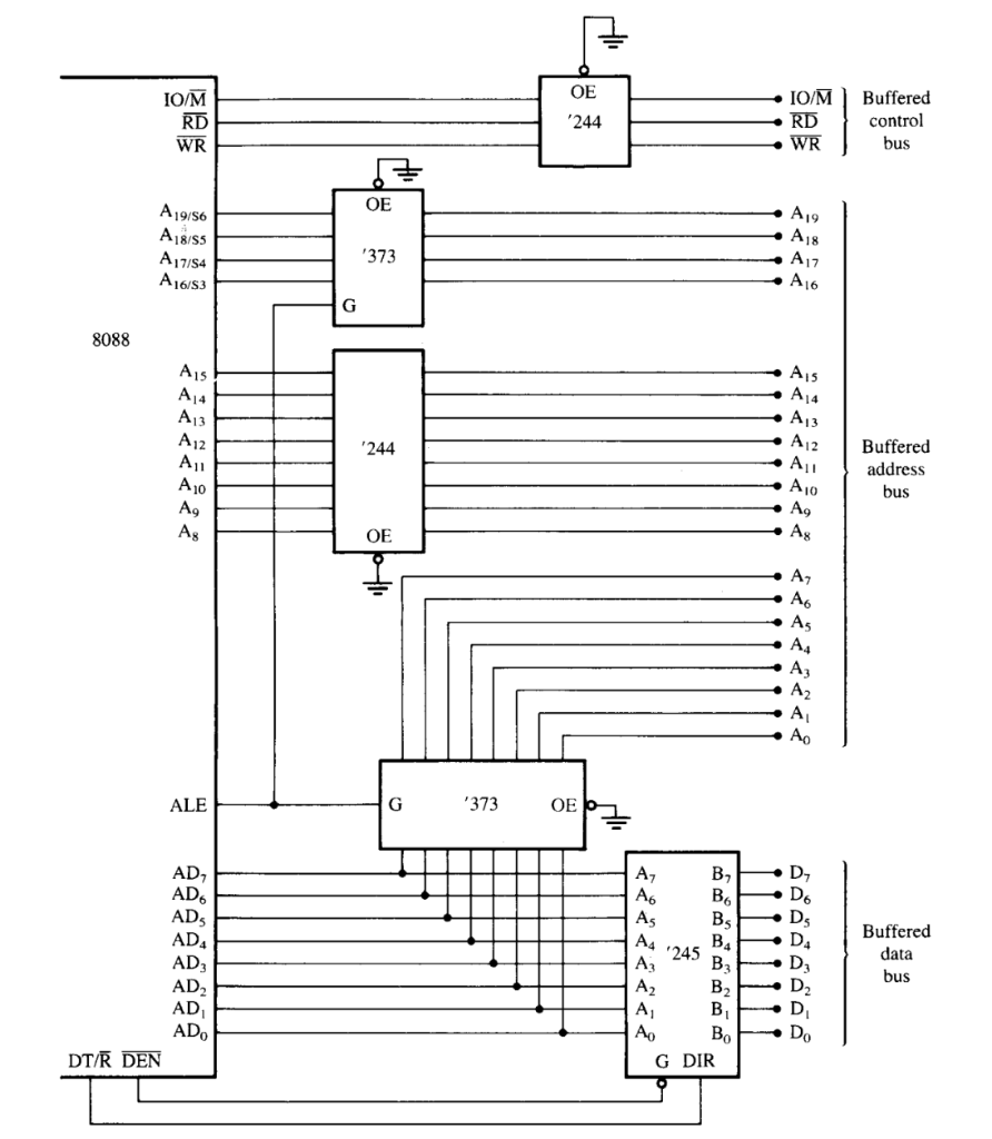
OE IO/M RD WR 244 IO/M RD WR Buffered control bus OE A19/56 A18/55 A 17/54 A 16/53 A19 A18 A17 A6 373 G 8088 ALS A14 A13 A12 ALL A 10 A, Ag Als A4 A13 A12 AL 244 Buffered address bus A10 Ag OE Ag A A6 - As A4 Az A2 A ALE G '373 OE AD AD AD AD AD AD AD A7 B AC B6 As A4 '245 , A2 B2 A B Ao G DIR B4 B3 D D D D4 D D2 D DO Buffered data bus AD DT/R DEN
Step by Step Solution
There are 3 Steps involved in it
Step: 1

Get Instant Access to Expert-Tailored Solutions
See step-by-step solutions with expert insights and AI powered tools for academic success
Step: 2

Step: 3
Ace Your Homework with AI
Get the answers you need in no time with our AI-driven, step-by-step assistance
Get Started
Database Concepts International Edition
Authors: David M. Kroenke
6th Edition International Edition
0133098222, 978-0133098228