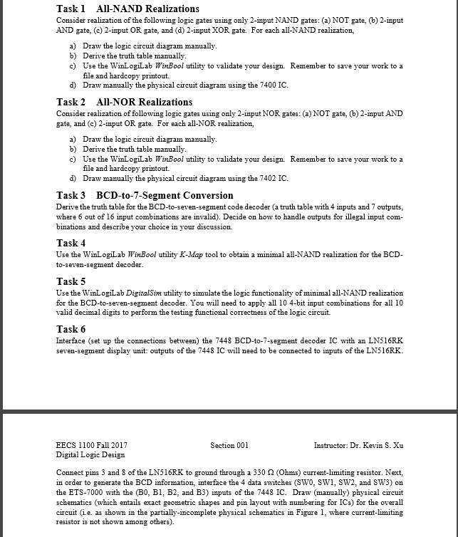
Task 1 All-NAND Realizations Consider realization of the following logic gates using only 2-input NAND gates: (a) NOT gate, (b) 2-input AND gate, (c) 2-input OR gate, and (d) 2-input XOR gate. For each all-NAND realization, a) Draw the logic circuit diagram manually b) Derive the truth table manually c Use the WinLogiLab WinBool utility to validate your design. Remember to save your work to a file and hardcopy printout. d) Drawmanually the physical circuit diagram using the 7400 IC. Task 2 AIl-NOR Realizations Consider realization of following logic gates using only 2-input NOR gates: (a) NOT gate, (b) 2-input AND gate, and (c) 2-input OR gate. For each all-NOR realization, a) Draw the logic circuit diagram manually b) Derive the truth table manually c) Use the WinLogiLab WinBool utility to validate your design. Remember to save your work to a file and hardcopy printout. d) Drawmanually the physical circuit diagram using the 7402 IC. Task 3 BCD-to-7-Segment Conversion Derive the truth table for the BCD-to-seven-segment code decoder (a truth table with 4 inputs and 7 outputs, where 6 out of 16 input combinations are invalid). Decide on how to handle outputs for illegal input com- binations and describe your choice in your Task 4 Use the WinLogiLab WinBool utility K-Map tool to obtain a minimal all-NAND realization for the BCD to-seven-segment decoder Task 5 Use the WinLogiLab DigitalSim utility to simulate the logic functionality of minimal all-NAND realization for the BCD-to-seven-segment decoder. You will need to apply all 10 4-bit input combinations for all 10 valid decimal digits to perform the testing functional correctness of the logic circuit Task 6 Interface (set up the connections between) the 7448 BCD-to-7-segment decoder IC with an LN516RK seven-segment display unit: outputs of the 7448 IC will need to be connected to inputs of the LN516RK Section 001 Instructor: Dr. Kevin S. Xu EECS 1100 Fall 2017 Digital Logic Design Connect pins 3 and 8 of the LN516RK to ground through a 330 (Ohms) current-limiting resistor. Next. in order to generate the BCD information, interface the 4 data switches (SW0, SWl, SW2, and SW3) on the ETS-7000 with the (B0, B1, B2, and B3) inputs of the 7448 IC. Draw (manually) physical circuit schematics (which entails exact geometric shapes and pin layout with numbering for ICs) for the overall circuit (ie. as shown in the partially-incomplete physical schematics in Figure 1, where current-limiting resistor is not shown among othrs). Task 1 All-NAND Realizations Consider realization of the following logic gates using only 2-input NAND gates: (a) NOT gate, (b) 2-input AND gate, (c) 2-input OR gate, and (d) 2-input XOR gate. For each all-NAND realization, a) Draw the logic circuit diagram manually b) Derive the truth table manually c Use the WinLogiLab WinBool utility to validate your design. Remember to save your work to a file and hardcopy printout. d) Drawmanually the physical circuit diagram using the 7400 IC. Task 2 AIl-NOR Realizations Consider realization of following logic gates using only 2-input NOR gates: (a) NOT gate, (b) 2-input AND gate, and (c) 2-input OR gate. For each all-NOR realization, a) Draw the logic circuit diagram manually b) Derive the truth table manually c) Use the WinLogiLab WinBool utility to validate your design. Remember to save your work to a file and hardcopy printout. d) Drawmanually the physical circuit diagram using the 7402 IC. Task 3 BCD-to-7-Segment Conversion Derive the truth table for the BCD-to-seven-segment code decoder (a truth table with 4 inputs and 7 outputs, where 6 out of 16 input combinations are invalid). Decide on how to handle outputs for illegal input com- binations and describe your choice in your Task 4 Use the WinLogiLab WinBool utility K-Map tool to obtain a minimal all-NAND realization for the BCD to-seven-segment decoder Task 5 Use the WinLogiLab DigitalSim utility to simulate the logic functionality of minimal all-NAND realization for the BCD-to-seven-segment decoder. You will need to apply all 10 4-bit input combinations for all 10 valid decimal digits to perform the testing functional correctness of the logic circuit Task 6 Interface (set up the connections between) the 7448 BCD-to-7-segment decoder IC with an LN516RK seven-segment display unit: outputs of the 7448 IC will need to be connected to inputs of the LN516RK Section 001 Instructor: Dr. Kevin S. Xu EECS 1100 Fall 2017 Digital Logic Design Connect pins 3 and 8 of the LN516RK to ground through a 330 (Ohms) current-limiting resistor. Next. in order to generate the BCD information, interface the 4 data switches (SW0, SWl, SW2, and SW3) on the ETS-7000 with the (B0, B1, B2, and B3) inputs of the 7448 IC. Draw (manually) physical circuit schematics (which entails exact geometric shapes and pin layout with numbering for ICs) for the overall circuit (ie. as shown in the partially-incomplete physical schematics in Figure 1, where current-limiting resistor is not shown among othrs)


