that's everything provides to me.
the scratched out part was asking us to look at this slide for help. thats all the information i can add to this question.
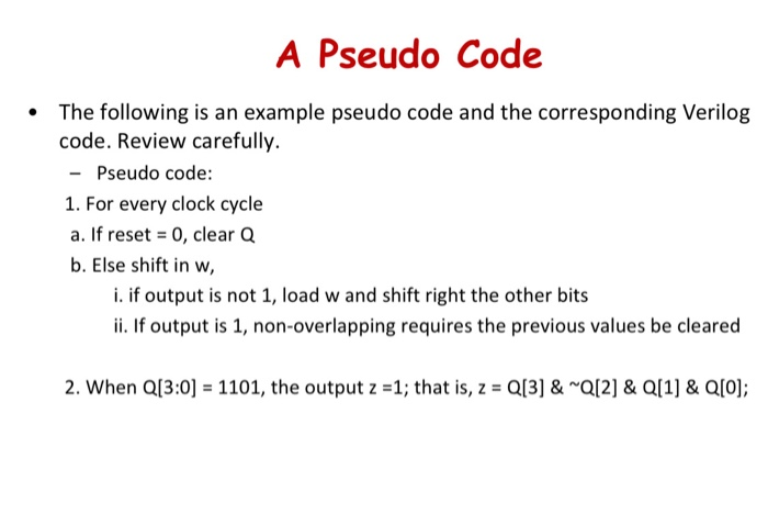
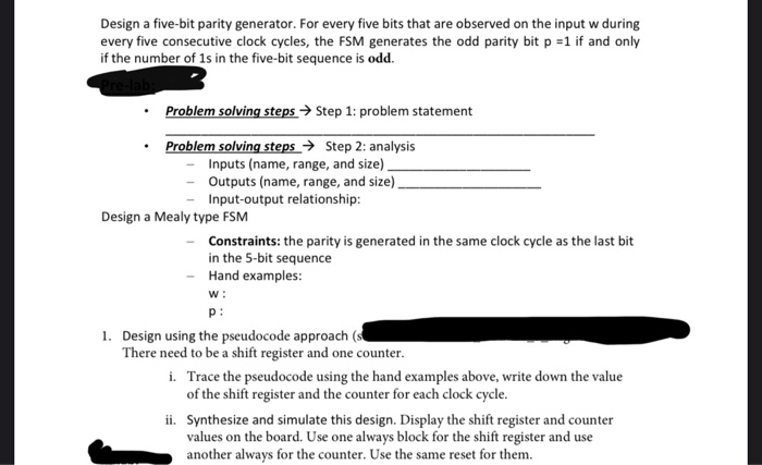
Design a five-bit parity generator. For every five bits that are observed on the input w during every five consecutive clock cycles, the FSM generates the odd parity bit p =1 if and only if the number of 1s in the five-bit sequence is odd. Problem solving steps Step 1: problem statement Problem solving steps Step 2: analysis - Inputs (name, range, and size) - Outputs (name, range, and size) - Input-output relationship: Design a Mealy type FSM Constraints: the parity is generated in the same clock cycle as the last bit in the 5-bit sequence Hand examples: W: p: 1. Design using the pseudocode approach (s There need to be a shift register and one counter. i. Trace the pseudocode using the hand examples above, write down the value of the shift register and the counter for each clock cycle. ii. Synthesize and simulate this design. Display the shift register and counter values on the board. Use one always block for the shift register and use another always for the counter. Use the same reset for them. A Pseudo Code The following is an example pseudo code and the corresponding Verilog code. Review carefully. - Pseudo code: 1. For every clock cycle a. If reset = 0, clear Q b. Else shift in w, i. if output is not 1, load w and shift right the other bits ii. If output is 1, non-overlapping requires the previous values be cleared 2. When Q[3:0) = 1101, the output z =1; that is, z = Q[3] & Q[2] & Q[1] & Q[0]; Design a five-bit parity generator. For every five bits that are observed on the input w during every five consecutive clock cycles, the FSM generates the odd parity bit p =1 if and only if the number of 1s in the five-bit sequence is odd. Problem solving steps Step 1: problem statement Problem solving steps Step 2: analysis - Inputs (name, range, and size) - Outputs (name, range, and size) - Input-output relationship: Design a Mealy type FSM Constraints: the parity is generated in the same clock cycle as the last bit in the 5-bit sequence Hand examples: W: p: 1. Design using the pseudocode approach (s There need to be a shift register and one counter. i. Trace the pseudocode using the hand examples above, write down the value of the shift register and the counter for each clock cycle. ii. Synthesize and simulate this design. Display the shift register and counter values on the board. Use one always block for the shift register and use another always for the counter. Use the same reset for them. A Pseudo Code The following is an example pseudo code and the corresponding Verilog code. Review carefully. - Pseudo code: 1. For every clock cycle a. If reset = 0, clear Q b. Else shift in w, i. if output is not 1, load w and shift right the other bits ii. If output is 1, non-overlapping requires the previous values be cleared 2. When Q[3:0) = 1101, the output z =1; that is, z = Q[3] & Q[2] & Q[1] & Q[0]