

Answered step by step
Verified Expert Solution
Question
1 Approved Answer
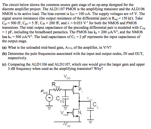
The circuit below shows the common source gain stage of an op-amp designed for the discrete amplifier project. The ALD1107 PMOS is the amplifying transistor
Step by Step Solution
There are 3 Steps involved in it
Step: 1

Get Instant Access to Expert-Tailored Solutions
See step-by-step solutions with expert insights and AI powered tools for academic success
Step: 2

Step: 3
Ace Your Homework with AI
Get the answers you need in no time with our AI-driven, step-by-step assistance
Get Started
Climate And Environmental Database Systems
Authors: Michael Lautenschlager ,Manfred Reinke
1st Edition
1461368332, 978-1461368335