Answered step by step
Verified Expert Solution
Question
1 Approved Answer
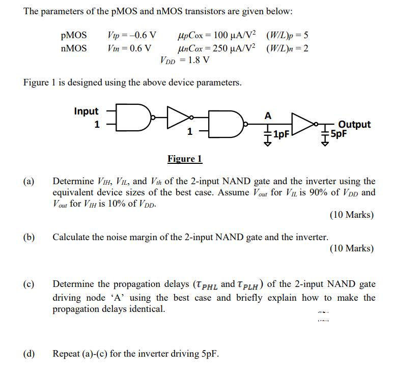
The parameters of the pMOS and nMOS transistors are given below: Vtp = -0.6 V UpCox= 100 A/V (W/L)p=5 unCox = 250 A/V (W/L)n

The parameters of the pMOS and nMOS transistors are given below: Vtp = -0.6 V UpCox= 100 A/V (W/L)p=5 unCox = 250 A/V (W/L)n = 2 Vtn = 0.6 V VDD = 1.8 V Figure 1 is designed using the above device parameters. (a) (b) (c) pMOS nMOS (d) Input 1 D AHH 1pF Repeat (a)-(c) for the inverter driving 5pF. Calculate the noise margin of the 2-input NAND gate and the inverter. Figure 1 Determine VIH, VIL, and Vth of the 2-input NAND gate and the inverter using the equivalent device sizes of the best case. Assume Vout for VI is 90% of VDD and Vout for VIH is 10% of VDD. (10 Marks) Output 5pF 13. Determine the propagation delays (TPHL and TPLH) of the 2-input NAND gate driving node 'A' using the best case and briefly explain how to make the propagation delays identical. (10 Marks)
Step by Step Solution
★★★★★
3.45 Rating (161 Votes )
There are 3 Steps involved in it
Step: 1
a For the 2input NAND gate assuming the best case and using the given device parameters VIL 09 18V 1...
Get Instant Access to Expert-Tailored Solutions
See step-by-step solutions with expert insights and AI powered tools for academic success
Step: 2

Step: 3

Ace Your Homework with AI
Get the answers you need in no time with our AI-driven, step-by-step assistance
Get Started


