Question
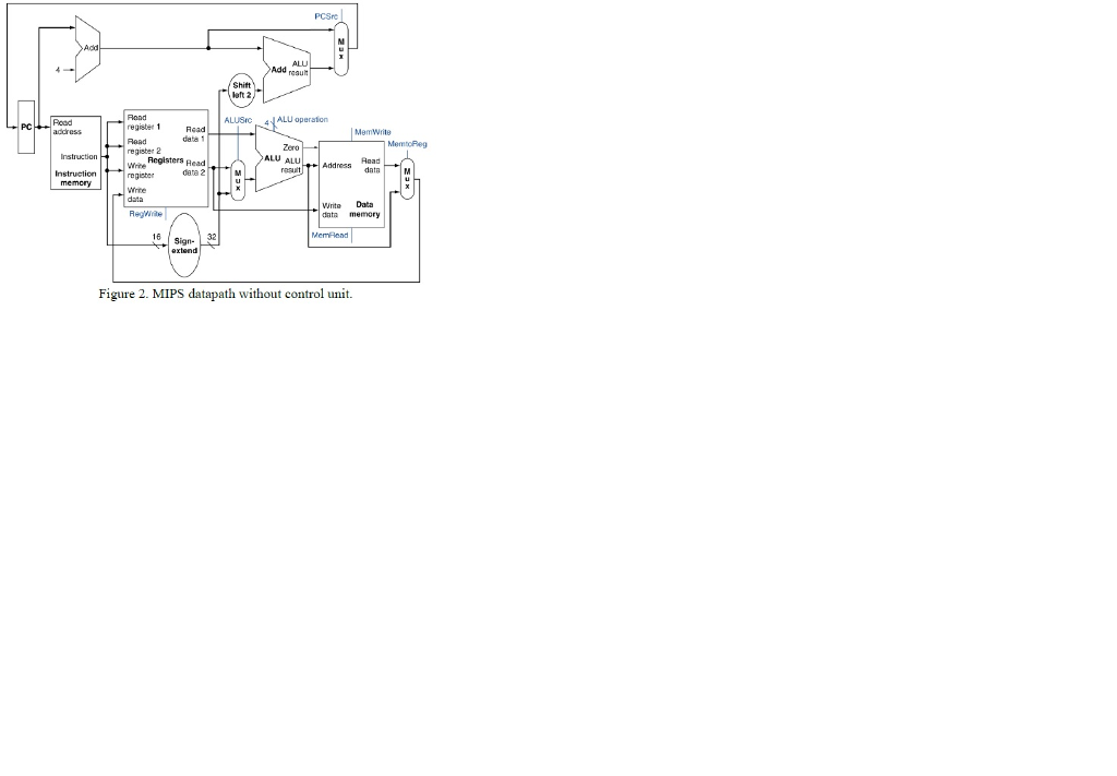
The figure shows a design of a MIPS processor which needs many additional blocks (e.g., control). Assume that the delay for each block in this
The figure shows a design of a MIPS processor which needs many additional blocks (e.g., control). Assume that the delay for each block in this design is as shown in the table below. I-MEM D-MEM Add Mux ALU Sign-Extend Shift-L-2 Regs 200ps 250ps 70ps 20ps 90ps 15ps 10ps 90ps (a) What is the minimum delay we will need to update the PC value to PC+4, and to read the instructions from memory? (b) Using the Figure 2 architecture, if we have just one instruction as unconditional PC-relative branch instruction, what is the minimum clock cycle for this processor? (Hint: for this instruction, you just need to find the blocks that you need for this instruction, and find the critical path from the PC to the end of that path). What is the minimum clock cycle time if we use the architecture in Figure 1 assuming the same unconditional PC-relative branch instruction? (c) Now consider the processor with all the set of instruction that we design the datapath for. What types of instruction will use Shift-Left-2 block? (d) Explain the ALUSrc signal. For what types of instructions ALUSrc is 1, and for what types it is 0?

Step by Step Solution
There are 3 Steps involved in it
Step: 1

Get Instant Access to Expert-Tailored Solutions
See step-by-step solutions with expert insights and AI powered tools for academic success
Step: 2

Step: 3

Ace Your Homework with AI
Get the answers you need in no time with our AI-driven, step-by-step assistance
Get Started


