Question
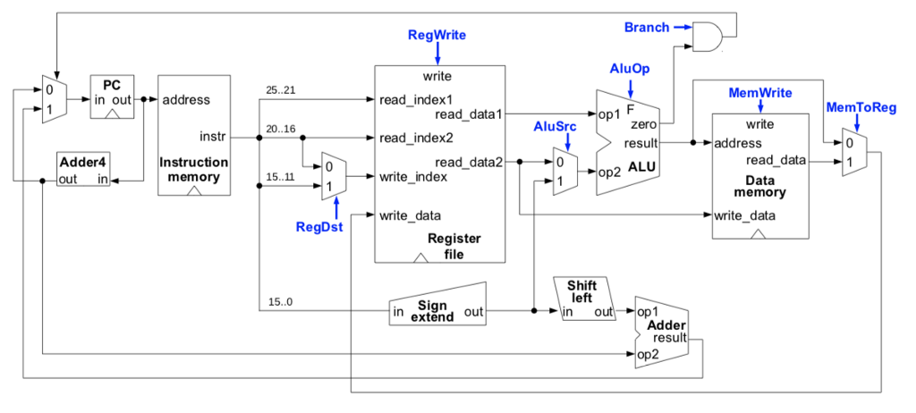
The following diagram represents the single-cycle datapath studied in class with support for a subset of the MIPS arithmetic-logic instructions, plus lw, sw, and beq.
The following diagram represents the single-cycle datapath studied in class with support for a subset of the MIPS arithmetic-logic instructions, plus lw, sw, and beq. Control signals appear highlighted in blue.

MIPS instruction j (jump) performs an unconditional jump to a destination address. The instruction is encoded using the J format, where field imm (bits 25..0) represents bits 27..2 of the target address (see MIPS reference card). Bits 1..0 of the target address are always 0, since the address of an instruction in memory is always a multiple of 4. Finally, bits 31..28 of the target address are taken directly from the 4 most significant bits of the current program counter (PC register).
a) Extend the datapath with support for instruction . Your circuit should include a new control signal named jump. When set, the new datapath elements should provide the required functionality. When not set, the datapath should behave exactly as it did before your extension.
You don't need to redraw the entire datapath. Focus only on the new datapath elements and connections, and draw only those components from the original datapath that are needed to understand the placement of your additions. For brevity, you can use labels to indicate the source or destination of wires connected to inputs and outputs of your new components. For example, if a wire comes from the instr output of the instruction memory, just label it InstructionMemory.instr. If a wire's destination is the input of the PC register, just label it PC.in.
b) List the value that each control signal should take when instruction j is decoded. Specify a value equal to X (don't care) whenever the value of a specific control signal does not matter, that is, when a value set to 0 or to 1 would not make any difference in the execution of instruction j.
Branch RegWrite AluOp write PC n outaddress 25..21 MemWrite read index1 MemToReg read data 1 op1 F 20..16 AluSrc zero write nstr read index2 address result read data Adder4 out in Instruction memory read data2 write index op2 ALU 15..11 Data memory write data write data RegDst Register file Shift left n o 15..0 in Sign op1 extend out Adder resu op2 Branch RegWrite AluOp write PC n outaddress 25..21 MemWrite read index1 MemToReg read data 1 op1 F 20..16 AluSrc zero write nstr read index2 address result read data Adder4 out in Instruction memory read data2 write index op2 ALU 15..11 Data memory write data write data RegDst Register file Shift left n o 15..0 in Sign op1 extend out Adder resu op2Step by Step Solution
There are 3 Steps involved in it
Step: 1

Get Instant Access to Expert-Tailored Solutions
See step-by-step solutions with expert insights and AI powered tools for academic success
Step: 2

Step: 3

Ace Your Homework with AI
Get the answers you need in no time with our AI-driven, step-by-step assistance
Get Started


