Answered step by step
Verified Expert Solution
Link Copied!

Question

1 Approved Answer

The thickness of photoresist applied to wafers in semiconductor manufacturing at a particular location on the wafer is uniformly distributed between 0.2002 and 0.2157 micrometers.
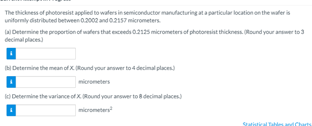
image text in transcribed
The thickness of photoresist applied to wafers in semiconductor manufacturing at a particular location on the wafer is uniformly distributed between 0.2002 and 0.2157 micrometers. (a) Determine the proportion of wafers that exceeds 0.2125 micrometers of photoresist thickness. (Round your answer to 3 decimal places.) i (b) Determine the mean of X. (Round your answer to 4 decimal places.) micrometers (c) Determine the variance of X. (Round your answer to 8 decimal places.) i micrometers? Statistical Tables and Charts

Step by Step Solution

There are 3 Steps involved in it

Step: 1

blur-text-image

Get Instant Access to Expert-Tailored Solutions

See step-by-step solutions with expert insights and AI powered tools for academic success

Step: 2

blur-text-image

Step: 3

blur-text-image

Ace Your Homework with AI

Get the answers you need in no time with our AI-driven, step-by-step assistance

Get Started

Recommended Textbook for

Calculus An Applied Approach

Authors: Ron Larson, Dennis J McKenzie, Larson/Edwards, Bruce H Edwards

7th Edition

1111809720, 9781111809720

More Books

Students also viewed these Mathematics questions