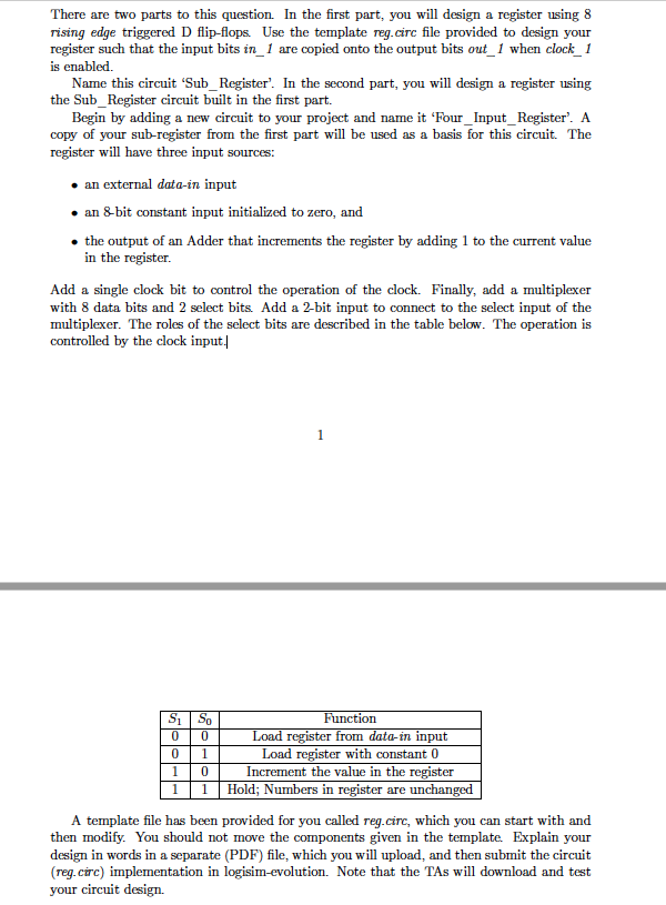
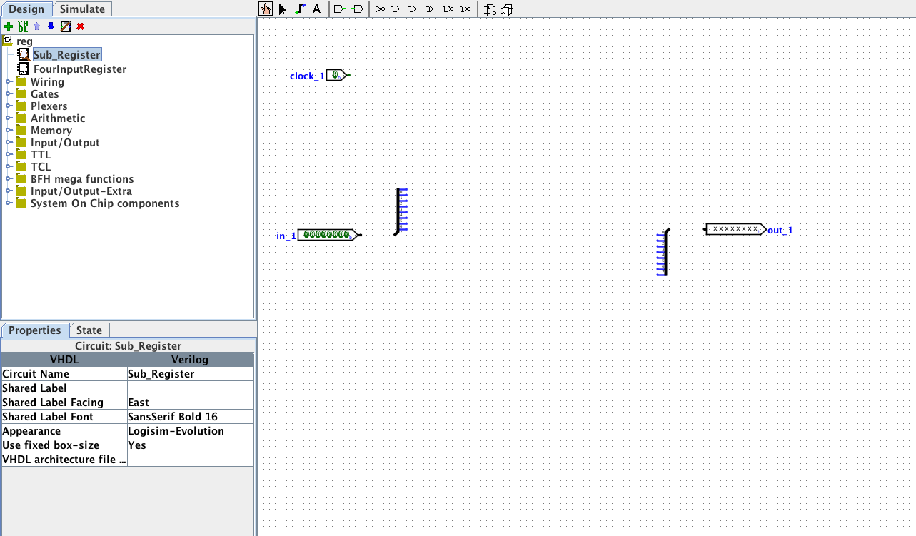
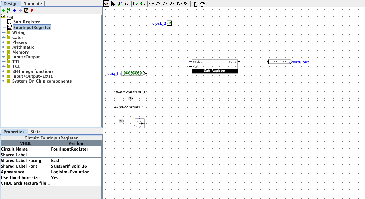
There are two parts to this question. In the first part, you will design a register using 8 rising edge triggered D flip-flops. Use the template reg.circ file provided to design your register such that the input bits in_1 are copied onto the output bits out_1 when clock_1 is enabled Name this circuit 'Sub_Register'. In the second part, you will design a register using the Sub_Register circuit built in the first part. Begin by adding a new circuit to your project and name it 'Four_Input_Register'. A copy of your sub-register from the first part will be used as a basis for this circuit. The register will have three input sources: an external data-in input an 8-bit constant input initialized to zero, and the output of an Adder that increments the register by adding 1 to the current value in the register. Add a single clock bit to control the operation of the clock. Finally, add a multiplexer with 8 data bits and 2 select bits. Add a 2-bit input to connect to the select input of the multiplexer. The roles of the select bits are described in the table below. The operation is controlled by the clock input. 10 Function Load register from data-in input Load register with constant 0 Increment the value in the register Hold; Numbers in register are unchanged 1 A template file has been provided for you called reg.circ, which you can start with and then modify. You should not move the components given in the template. Explain your design in words in a separate (PDF) file, which you will upload, and then submit the circuit (reg.circ) implementation in logisim-evolution. Note that the TAs will download and test your circuit design. ANSAD-DDODD D DO DO clock 10 0 0 Design Simulate + 8 + + 2 * El reg Sub_Register Fourinput Register Wiring Gates Plexers Arithmetic Memory Input/Output TTL TCL BFH mega functions Input/Output-Extra System On Chip components 0 0 0 0 0 0 0 0 0 LLLLLLL 00000000 Properties State Circuit: Sub_Register VHDL Verilog Circuit Name Sub_Register Shared Label Shared Label Facing Shared Label Font Sans Serif Bold 16 Appearance Logisim-Evolution Use fixed box-size Yes VHDL architecture file ... AR SAD-DDD D D D D 119 clock_20 9 9 Design Simulate + 8 + + 2 * Dreg Sub_Register FourlnputRegister Wiring Gates Plexers Arithmetic Memory Input/Output TTL TCL BFH mega functions Input/Output-Extra System On Chip components 9 9 9 9 9 9 9 Sub_Register data_in_00000000 9 9 8-bit constant 0 00. 8-bit constant i 81. ::: Properties State Circuit: FourinputRegister VHDL Verilog Circuit Name FourlnputRegister Shared Label Shared Label Facing East Shared Label Font Sans Serif Bold 16 Appearance Logisim-Evolution Use fixed box-size Yes VHDL architecture file ... There are two parts to this question. In the first part, you will design a register using 8 rising edge triggered D flip-flops. Use the template reg.circ file provided to design your register such that the input bits in_1 are copied onto the output bits out_1 when clock_1 is enabled Name this circuit 'Sub_Register'. In the second part, you will design a register using the Sub_Register circuit built in the first part. Begin by adding a new circuit to your project and name it 'Four_Input_Register'. A copy of your sub-register from the first part will be used as a basis for this circuit. The register will have three input sources: an external data-in input an 8-bit constant input initialized to zero, and the output of an Adder that increments the register by adding 1 to the current value in the register. Add a single clock bit to control the operation of the clock. Finally, add a multiplexer with 8 data bits and 2 select bits. Add a 2-bit input to connect to the select input of the multiplexer. The roles of the select bits are described in the table below. The operation is controlled by the clock input. 10 Function Load register from data-in input Load register with constant 0 Increment the value in the register Hold; Numbers in register are unchanged 1 A template file has been provided for you called reg.circ, which you can start with and then modify. You should not move the components given in the template. Explain your design in words in a separate (PDF) file, which you will upload, and then submit the circuit (reg.circ) implementation in logisim-evolution. Note that the TAs will download and test your circuit design. ANSAD-DDODD D DO DO clock 10 0 0 Design Simulate + 8 + + 2 * El reg Sub_Register Fourinput Register Wiring Gates Plexers Arithmetic Memory Input/Output TTL TCL BFH mega functions Input/Output-Extra System On Chip components 0 0 0 0 0 0 0 0 0 LLLLLLL 00000000 Properties State Circuit: Sub_Register VHDL Verilog Circuit Name Sub_Register Shared Label Shared Label Facing Shared Label Font Sans Serif Bold 16 Appearance Logisim-Evolution Use fixed box-size Yes VHDL architecture file ... AR SAD-DDD D D D D 119 clock_20 9 9 Design Simulate + 8 + + 2 * Dreg Sub_Register FourlnputRegister Wiring Gates Plexers Arithmetic Memory Input/Output TTL TCL BFH mega functions Input/Output-Extra System On Chip components 9 9 9 9 9 9 9 Sub_Register data_in_00000000 9 9 8-bit constant 0 00. 8-bit constant i 81. ::: Properties State Circuit: FourinputRegister VHDL Verilog Circuit Name FourlnputRegister Shared Label Shared Label Facing East Shared Label Font Sans Serif Bold 16 Appearance Logisim-Evolution Use fixed box-size Yes VHDL architecture file