Answered step by step
Verified Expert Solution
Question
1 Approved Answer
Upon completion of this lab you should be able to create and test a design using the Xilinx ISE tools. 2 General This lab
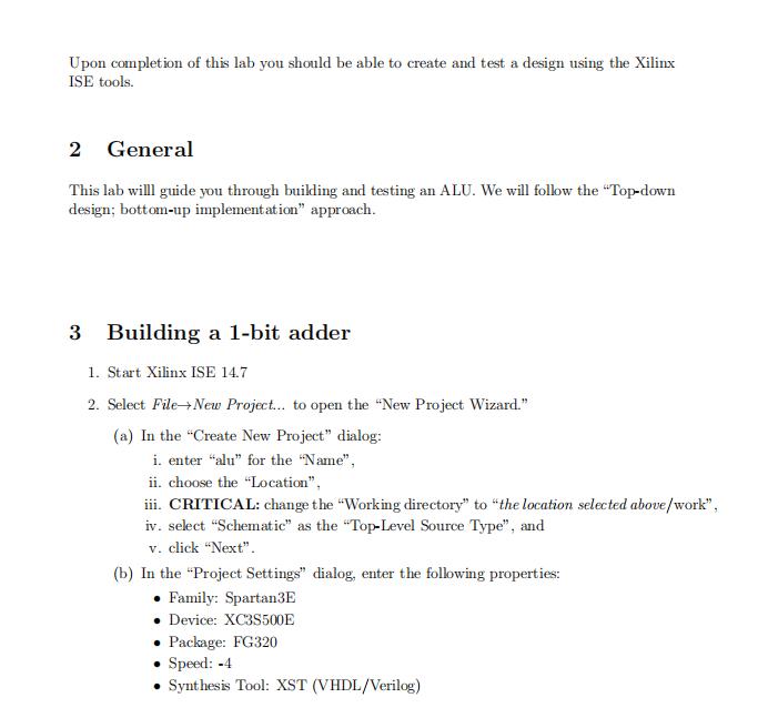


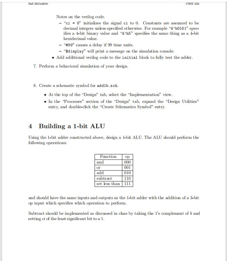
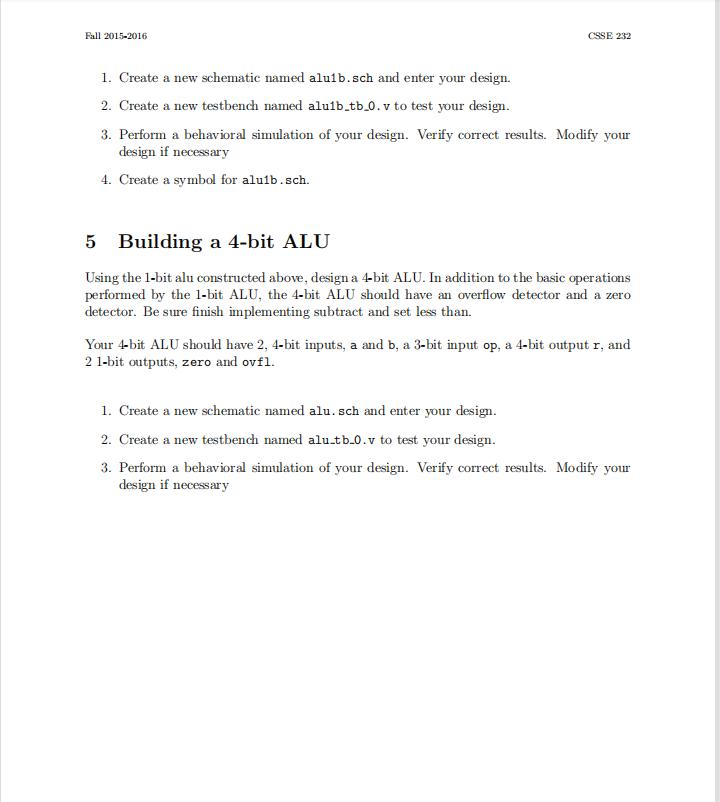
Upon completion of this lab you should be able to create and test a design using the Xilinx ISE tools. 2 General This lab willl guide you through building and testing an ALU. We will follow the "Top-down design: bottom-up implementation" approach. 3 Building a 1-bit adder 1. Start Xilinx ISE 14.7 2. Select FileNew Project... to open the "New Project Wizard." (a) In the "Create New Project" dialog: i. enter "alu" for the "Name", ii. choose the "Location", iii. CRITICAL: change the "Working directory" to "the location selected above/work", iv. select "Schematic" as the "Top-Level Source Type", and v. click "Next". (b) In the "Project Settings" dialog, enter the following properties: Family: Spartan3E Device: XC3S500E Package: FG320 Speed: -4 Synthesis Tool: XST (VHDL/Verilog) Fall 2015-2016 Simulator: ISim (VHDL/Verilog) Prefered Language: Verilog and click "Next". (c) Click "Finish" in the "Project Summary" dialog. Note: You can change the project properties by right clicking on the device (i.e. xc3s500e-4fg320) in the "Hierarchy" section of the "Design" tab and selecting "De- sign Properties..." CSSE 232 3. Add a new source to the project. There are a number of ways that you can do this: Right click on the device in the "Hierarchy" section of the "Design" tab and select "New Source..." Select Project New Source... . Click the "New Source" icon in the toolbar. The "New Source Wizard" should appear. (a) In the "Select Source Type" dialog, select "Schematic", enter "add1b" as the "File name:" and click "Next". (b) In the "Summary" dialog, click "Finish". 4. In add1b.sch implement the following logic: r=ci-a-b+ci-a-l and -b+ciab+ci-a-b (1) co= ci-a +ci-b+ab, (2) where a and b are inputs to the adder, ci is the carry-in, r is the result, and co is the carry-out. You should build the logic using and gates, or gates and inverters, which are all available in the symbols tab. To search for a symbol, type the first part of a symbols name in the "Symbol Name Filter". To add a symbol to your schematic, select a symbol in the symbol pane (this will switch to "add symbol" mode) and click in the schematic. Clicking again will place another symbol. Pushing "Esc" or right-clicking will cancel "add symbol" mode. To connect the symbols click the "Add Wire" icon in the toolbar. Click and drag in the schematic to specify a wire between a single pair of points. Use clicks (no drag) to specify a sequence of connected wire points. Double click will terminate the sequence. To add input and output pins click the "Add I/O Marker" icon in the toolbar. To name the input and output pins, click the "Add Net Name" icon in the toolbar and fill in "Name" in the "Options" pane. To check your schematic click "Check Schematic" from the toolbar. Try to create your own design. However, if you get stuck, you can take a look at mine. 5. Make sure addib. sch is set as the top level module and synthesize it. Correct any errors. 6. Create a testbench. (a) At the top of the "Design" tab, select the "Simulation" view. (b) Add a new source to the project. For source type select "Verilog Test Fixture" and filename add1b_tb_0. On the "Associate Source" dialog select "add1b" and click "Next". Click "Finish". (c) In the "Hierarchy" section of the "Design" tab, double-click on add1b_tb_0. vand examine the test bench. (d) Edit the verilog code to fully test the adder. Feel free to change the module name to something more reasonable. I used add1b_tb_0. 15 October 2015 Delete the following section. 'ifdef auto_init initial begin ci = 0; b = 0; a = 0; 'endif Add the following section in its place. initial begin ci = 0; b = 0; a = 0; // Wait 100ns for the simulator to finish initializing # 100; a = 1; #1; if ((r == 1) && (co == 0)) $display("okay 1"); $display("fail 1"); end else Page 3 Fall 2015-2016 Notes on the verilog code. - "ci = 0" initializes the signal ci to 0. Constants are assumed to be decimal integers unless specified otherwise. For example "4'b0101" spec- ifies a 4-bit binary value and "4'h5" specifies the same thing as a 4-bit hexidecimal value. - "# 99" causes a delay if 99 time units. - "$display" will print a message on the simulation console. Add additional verilog code to the initial block to fully test the adder. 7. Perform a behavioral simulation of your design. 8. Create a schematic symbol for add1b.sch. At the top of the "Design" tab, select the "Implementation" view. . In the Processes" section of the "Design" tab, expand the "Design Utilities" entry, and double-click the "Create Schematics Symbol" entry. CSSE 232 4 Building a 1-bit ALU Using the 1-bit adder constructed above, design a 1-bit ALU. The ALU should perform the following operations: Function and or add op 000 001 010 subtract 110 set less than 111 and should have the same inputs and outputs as the 1-bit adder with the addition of a 3-bit op input which specifies which operation to perform. Subtract should be implemented as discussed in class by taking the I's complement of b and setting ci of the least significant bit to a 1. Fall 2015-2016 1. Create a new schematic named alulb.sch and enter your design. 2. Create a new testbench named alulb_tb_0. v to test your design. CSSE 232 3. Perform a behavioral simulation of your design. Verify correct results. Modify your design if necessary 4. Create a symbol for aluib.sch. 5 Building a 4-bit ALU Using the 1-bit alu constructed above, design a 4-bit ALU. In addition to the basic operations performed by the 1-bit ALU, the 4-bit ALU should have an overflow detector and a zero detector. Be sure finish implementing subtract and set less than. Your 4-bit ALU should have 2, 4-bit inputs, a and b, a 3-bit input op, a 4-bit output r, and 2 1-bit outputs, zero and ovfl. 1. Create a new schematic named alu. sch and enter your design. 2. Create a new testbench named alu_tb_0.v to test your design. 3. Perform a behavioral simulation of your design. Verify correct results. Modify your design if necessary
Step by Step Solution
★★★★★
3.41 Rating (154 Votes )
There are 3 Steps involved in it
Step: 1
Sol Truth fable A J A B 1 1 1 bit full Adder A...
Get Instant Access to Expert-Tailored Solutions
See step-by-step solutions with expert insights and AI powered tools for academic success
Step: 2

Step: 3

Ace Your Homework with AI
Get the answers you need in no time with our AI-driven, step-by-step assistance
Get Started


