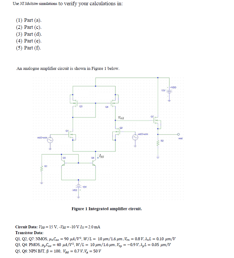
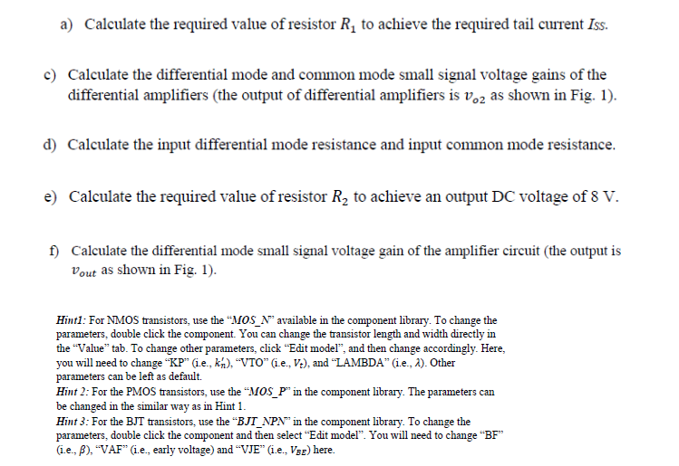
Use NI Multsim simulations to verify your calculations in: (1) Part (a). (2) Part (0) (3) Part (d). (4) Part (e). (5) Part (f). An analogue amplifier circuit is shown in Figure 1 below. VDD 15V Q3 04 Vo2 01 videvam vd2 + H. vout R2 Q5 as! Iss R1 10V VEE Figure 1 Integrated amplifier circuit. Circuit Data: Vpp = 15 V, -Ves =-10 V Iss=2.0 mA Transistor Data: Q1, Q2, Q7: NMOS, un Cox = 90 A/V2, W/L = 10 um/1.6 um, Vin = 0.8V, An L = 0.10 um/V 03. 04: PMOS, Hp Cox = 40 uA/V2, W/L = 10 um/1.6 um, Vtp =-0.9V,1,L = 0.05 um/V Q5, Q6: NPN BJT, B = 100, VBE = 0.7 V,VA= 50 V a) Calculate the required value of resistor R, to achieve the required tail current Iss. c) Calculate the differential mode and common mode small signal voltage gains of the differential amplifiers (the output of differential amplifiers is v.2 as shown in Fig. 1). d) Calculate the input differential mode resistance and input common mode resistance. e) Calculate the required value of resistor R, to achieve an output DC voltage of 8 V. f) Calculate the differential mode small signal voltage gain of the amplifier circuit (the output is Vout as shown in Fig. 1). Hinti: For NMOS transistors, use the "MOS_N" available in the component library. To change the parameters, double click the component. You can change the transistor length and width directly in the "Value" tab. To change other parameters, click Edit model, and then change accordingly. Here, you will need to change "KP" (1.e., kh). "VTO" (i.e., V:), and LAMBDA" (i.e., 1). Other parameters can be left as default Hint 2: For the PMOS transistors, use the "MOS_P" in the component library. The parameters can be changed in the similar way as in Hint 1. Hint 3: For the BJT transistors, use the BJT_NPN" in the component library. To change the parameters, double click the component and then select Edit model. You will need to change "BF" (1.e., B), VAF (1.e., early voltage) and VJE (1.e., Vse) here. Use NI Multsim simulations to verify your calculations in: (1) Part (a). (2) Part (0) (3) Part (d). (4) Part (e). (5) Part (f). An analogue amplifier circuit is shown in Figure 1 below. VDD 15V Q3 04 Vo2 01 videvam vd2 + H. vout R2 Q5 as! Iss R1 10V VEE Figure 1 Integrated amplifier circuit. Circuit Data: Vpp = 15 V, -Ves =-10 V Iss=2.0 mA Transistor Data: Q1, Q2, Q7: NMOS, un Cox = 90 A/V2, W/L = 10 um/1.6 um, Vin = 0.8V, An L = 0.10 um/V 03. 04: PMOS, Hp Cox = 40 uA/V2, W/L = 10 um/1.6 um, Vtp =-0.9V,1,L = 0.05 um/V Q5, Q6: NPN BJT, B = 100, VBE = 0.7 V,VA= 50 V a) Calculate the required value of resistor R, to achieve the required tail current Iss. c) Calculate the differential mode and common mode small signal voltage gains of the differential amplifiers (the output of differential amplifiers is v.2 as shown in Fig. 1). d) Calculate the input differential mode resistance and input common mode resistance. e) Calculate the required value of resistor R, to achieve an output DC voltage of 8 V. f) Calculate the differential mode small signal voltage gain of the amplifier circuit (the output is Vout as shown in Fig. 1). Hinti: For NMOS transistors, use the "MOS_N" available in the component library. To change the parameters, double click the component. You can change the transistor length and width directly in the "Value" tab. To change other parameters, click Edit model, and then change accordingly. Here, you will need to change "KP" (1.e., kh). "VTO" (i.e., V:), and LAMBDA" (i.e., 1). Other parameters can be left as default Hint 2: For the PMOS transistors, use the "MOS_P" in the component library. The parameters can be changed in the similar way as in Hint 1. Hint 3: For the BJT transistors, use the BJT_NPN" in the component library. To change the parameters, double click the component and then select Edit model. You will need to change "BF" (1.e., B), VAF (1.e., early voltage) and VJE (1.e., Vse) here