

Answered step by step
Verified Expert Solution
Question
1 Approved Answer
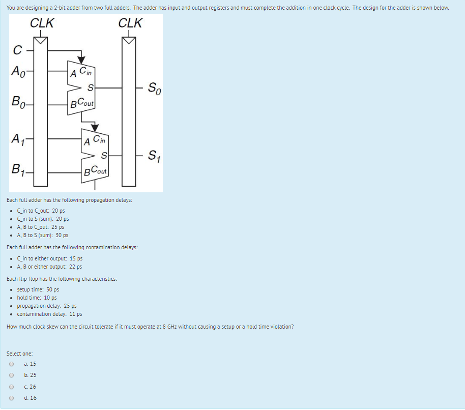
You are designing a 2-bit adder from two full adders. The adder has input and output registers and must complete the addition in one clock
Step by Step Solution
There are 3 Steps involved in it
Step: 1

Get Instant Access to Expert-Tailored Solutions
See step-by-step solutions with expert insights and AI powered tools for academic success
Step: 2

Step: 3
Ace Your Homework with AI
Get the answers you need in no time with our AI-driven, step-by-step assistance
Get Started
Oracle 10g SQL
Authors: Joan Casteel, Lannes Morris Murphy
1st Edition
141883629X, 9781418836290