

Question: Assume the inputs (A, B, C), and (D) to the circuit in Figure P17.16 are either 0 or (2.5 mathrm{~V}). Let the (mathrm{B}-mathrm{E}) turn-on voltage
Assume the inputs \(A, B, C\), and \(D\) to the circuit in Figure P17.16 are either 0 or \(2.5 \mathrm{~V}\). Let the \(\mathrm{B}-\mathrm{E}\) turn-on voltage be \(0.7 \mathrm{~V}\) for both the npn and pnp transistors. Assume \(\beta=150\) for the npn devices and \(\beta=90\) for the pnp devices.
(a) Determine the voltage at \(Y\) for: (i) \(A=B=C=D=0\); (ii) \(A=B=0, C=D=2.5 \mathrm{~V}\); and (iii) \(A=C=2.5 \mathrm{~V}, B=D=0\).
(b) What logic function does this circuit implement?
(c) Determine the power dissipated in the circuit for the conditions given in part (a).
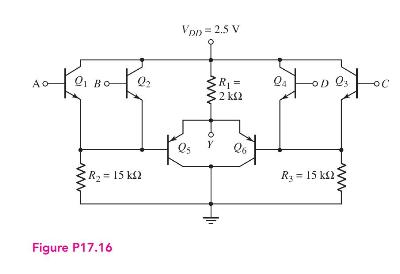
A Q BO Q2 VDD = 2.5 V ww R = 2 R = 15 k$2 Q6 Figure P17.16 Q4 OD 23 R = 15 k
Step by Step Solution
3.46 Rating (149 Votes )
There are 3 Steps involved in it
FULL SOLUTION Step 1 Introduction Overview In this question inputs A B C and Dall of which are either 0 or 25 voltsare used to analyze a transistorbas... View full answer

Get step-by-step solutions from verified subject matter experts