

Question: Consider the circuit shown in Figure P4.70. The transistor parameters are (V_{T P 1}=-0.4 mathrm{~V}, quad V_{T N 2}=0.4 mathrm{~V}, quad(W / L)_{1}=20, quad(W /
Consider the circuit shown in Figure P4.70. The transistor parameters are \(V_{T P 1}=-0.4 \mathrm{~V}, \quad V_{T N 2}=0.4 \mathrm{~V}, \quad(W / L)_{1}=20, \quad(W / L)_{2}=80\), \(k_{p}^{\prime}=40 \mu \mathrm{A} / \mathrm{V}^{2}, k_{n}^{\prime}=100 \mu \mathrm{A} / \mathrm{V}^{2}\), and \(\lambda_{1}=\lambda_{2}=0\). Let \(R_{\text {in }}=200 \mathrm{k} \Omega\).
(a) Design the circuit such that \(I_{D Q 1}=0.1 \mathrm{~mA}, \quad I_{D Q 2}=0.3 \mathrm{~mA}\), \(V_{S D Q 1}=1.0 \mathrm{~V}\), and \(V_{D S Q 2}=2.0 \mathrm{~V}\). The voltage across \(R_{S 1}\) is to be \(0.6 \mathrm{~V}\).
(b) Determine the small-signal voltage gain \(A_{v}=v_{o} / v_{i}\).
(c) Find the smallsignal output resistance \(R_{o}\).
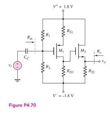
Vi +1 Rin HH Cc ww ww R V+= 1.8 V R$1 M M R R$2 RDl Figure P4.70 V = -1.8 V
Step by Step Solution
3.33 Rating (156 Votes )
There are 3 Steps involved in it

Get step-by-step solutions from verified subject matter experts