

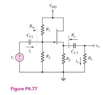
Question: Consider the source-follower JFET amplifier in Figure P4.77 with transistor parameters (I_{D S S}=10 mathrm{~mA}, V_{P}=-5 mathrm{~V}), and (lambda=0.01 mathrm{~V}^{-1}). Let (V_{D D}=12 mathrm{~V}) and
Consider the source-follower JFET amplifier in Figure P4.77 with transistor parameters \(I_{D S S}=10 \mathrm{~mA}, V_{P}=-5 \mathrm{~V}\), and \(\lambda=0.01 \mathrm{~V}^{-1}\). Let \(V_{D D}=12 \mathrm{~V}\) and \(R_{L}=0.5 \mathrm{k} \Omega\).
(a) Design the circuit such that \(R_{\text {in }}=100 \mathrm{k} \Omega\), and the \(Q\)-point is at \(I_{D Q}=I_{D S S} / 2\) and \(V_{D S Q}=V_{D D} / 2\).
(b) Determine the resulting small-signal voltage gain \(A_{v}=v_{o} / v_{i}\) and the output resistance \(R_{o}\).
Rin CC1 +1 VDD R www ww R Figure P4.77 Ro CC2 RL Rs ww
Step by Step Solution
3.44 Rating (160 Votes )
There are 3 Steps involved in it
a RS12 mathrmk Ome... View full answer

Get step-by-step solutions from verified subject matter experts