

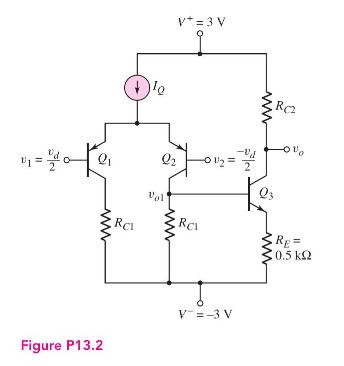
Design the circuit in Figure 13.2 such that the maximum power dissipated in the circuit is (15
Question:
Design the circuit in Figure 13.2 such that the maximum power dissipated in the circuit is \(15 \mathrm{~mW}\) and such that the common-mode input voltage is in the range \(-3 \leq v_{C M} \leq 3 \mathrm{~V}\). Using a computer simulation, adjust the value of \(R_{3}\) such that the output voltage is zero for zero input signal voltages.
Fantastic news! We've Found the answer you've been seeking!
Step by Step Answer:

Answered By
Vikash Gupta
I am graduated in Physics in 2018, from KIRORIMAL COLLEGE, University of Delhi. Now I am persuing Master's degree in physics. I like to do physics problems. I have experience of 1 year in tutoring. I think Physics is the only subject where you understand things,how they are happening . In physics you learn Maths and apply it. So I would like to join your platform to solve many Physics problems.
5+ Reviews
10+ Question Solved
Related Book For 

Microelectronics Circuit Analysis And Design
ISBN: 9780071289474
4th Edition
Authors: Donald A. Neamen
Question Posted:
