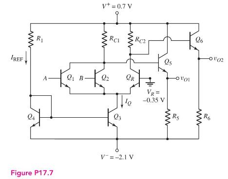
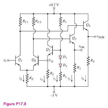
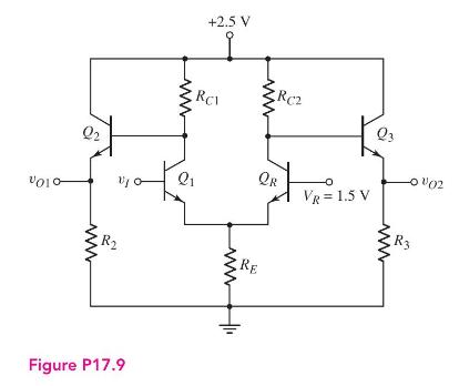
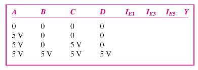
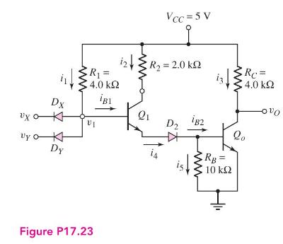
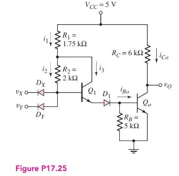
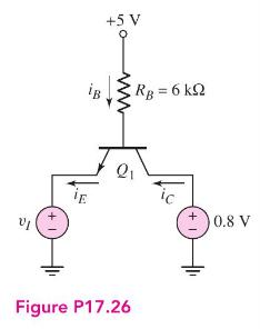
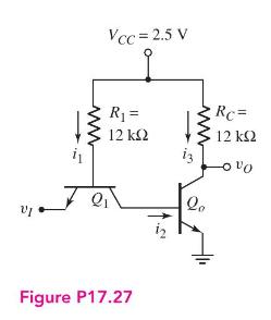
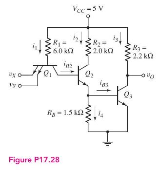
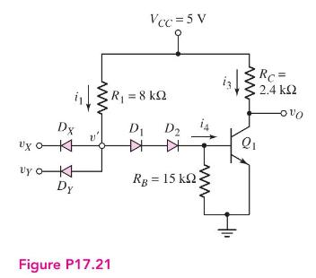
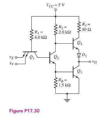
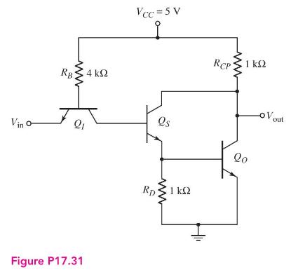
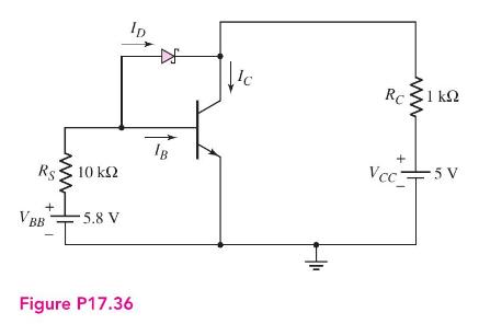
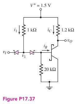
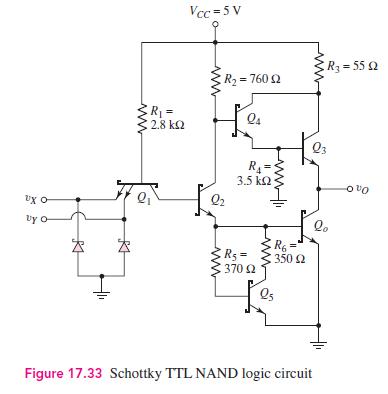
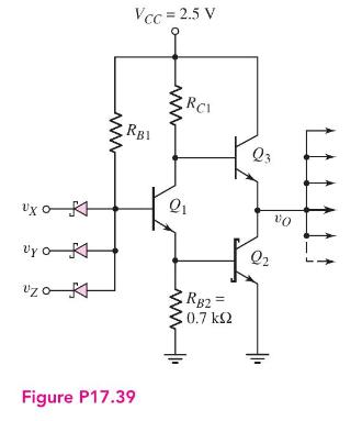
All Matches
Solution Library
Expert Answer
Textbooks
Search Textbook questions, tutors and Books
Oops, something went wrong!
Change your search query and then try again
Toggle navigation
FREE Trial
S
Books
FREE
Tutors
Study Help
Expert Questions
Accounting
General Management
Mathematics
Finance
Organizational Behaviour
Law
Physics
Operating System
Management Leadership
Sociology
Programming
Marketing
Database
Computer Network
Economics
Textbooks Solutions
Accounting
Managerial Accounting
Management Leadership
Cost Accounting
Statistics
Business Law
Corporate Finance
Finance
Economics
Auditing
Ask a Question
Search
Search
Sign In
Register
study help
computer science
systems analysis and design 12th
Questions and Answers of
Systems Analysis And Design 12th
Sketch the circuit configuration and discuss the operation of the basic ECL circuit.
Why must emitter-follower output stages be added to the diff-amp to make this circuit a practical logic gate?
Sketch a modified ECL circuit in which a Schottky diode is incorporated in the collector portion of the circuit. Explain the purpose of the Schottky diode.
Explain the concept of series gating for ECL circuits. What are the advantages of this configuration?
Sketch a diode-transistor NAND circuit and explain the operation of the circuit. Explain the concept of minimum \(\beta\) and the purpose of the pull-down resistor.
Explain the operation and purpose of the input transistor in a TTL circuit.
Sketch a basic TTL NAND circuit and explain its operation.
Sketch a totem-pole output stage and explain its operation and the advantages of incorporating this circuit in the TTL circuit.
Explain how maximum fanout can be based on maintaining the output transistor in saturation when the output is low.
Explain how maximum fanout can be based on a maximum rated collector current in the output transistor when the output is low.
Explain the operation of a Schottky clamped transistor. What are its advantages?
What is the primary advantage of a Schottky TTL NAND gate compared to a regular TTL NAND gate.
Sketch a low-power Schottky TTLNAND circuit. What are the primary differences between this circuit and the regular DTL circuit considered earlier in the chapter?
Sketch a basic BiCMOS inverter and explain its operation. Explain the advantages of this inverter compared to a simple CMOS inverter.
For the differential amplifier circuit in Figure P17.1, neglect the base currents. (a) Determine \(R_{C}\) such that \(v_{O 1}=v_{O 2}=-0.2 \mathrm{~V}\) when \(v_{1}=-0.7 \mathrm{~V}\). (b) Using
Neglect base currents in the circuit in Figure P17.2. (a) Determine \(R_{E}\) and \(R_{C}\) such that \(i_{E}=80 \mu \mathrm{A}\) and \(v_{O 1}=v_{O 2}=-0.25 \mathrm{~V}\) when \(v_{1}=-1.0
Neglect base currents in the circuit in Figure P17.3. (a) Determine the value of \(R_{C 2}\) such that the minimum value of \(v_{O 2}=0\). (b) Determine the value of \(R_{C 1}\) such that \(v_{O 1}=1
For the circuit in Figure P17.3, \(R_{C 1}=R_{C 2}=1 \mathrm{k} \Omega\). Determine \(v_{O 1}\) and \(v_{O 2}\) for (a) \(v_{I}=0.5 \mathrm{~V}\) and (b) \(v_{I}=-0.5 \mathrm{~V}\). Neglect base
Consider the circuit in Figure P17.5. (a) Determine \(R_{C 2}\) such that \(v_{2}=\) \(-1 \mathrm{~V}\) when \(Q_{2}\) is on and \(Q_{1}\) is off. (b) For \(v_{\text {in }}=-0.7\), determine \(R_{C
Consider the ECL logic circuit in Figure P17.6. Neglect base currents. (a) Determine the reference voltage \(V_{R}\). (b) Find the logic 0 and logic 1 voltage values at each output \(v_{O 1}\) and
Consider the circuit in Figure P17.7. (a) Determine \(R_{1}\) such that \(I_{\mathrm{REF}}=0.20 \mathrm{~mA}\). (b) Determine the values of \(R_{5}\) and \(R_{6}\) such that the maximum currents in
Consider the circuit in Figure P17.8. Neglect base currents. Determine all resistor values such that the following specifications are satisfied: logic \(1=0 \mathrm{~V}\) and logic \(0=-1.0
In the ECL circuit in Figure P17.9, the outputs have a logic swing of \(0.60 \mathrm{~V}\), which is symmetrical about the reference voltage. Neglect base currents. The maximum emitter current for
For the circuit in Figure P17.10, complete the following table. What logic function does the circuit perform? A 0 B C D IEL 5 V 5 V 5 V 100s 0 0 0 0 5 V 0 5 V 5 V 5 V JE3 IES Y 13
Consider the ECL circuit in Figure P17.11. The input voltages \(A\) and \(B\) are compatible with the output voltages \(v_{O 1}\) and \(v_{O 2}\). (a) Determine the reference voltage \(V_{R}\). (b)
A positive-voltage-supply ECL logic gate is shown in Figure P17.12. Neglect base currents.(a) What logic function is performed by this circuit.(b) What are the logic 1 and logic 0 values of \(v_{2}\)
In the circuit in Figure P17.13, the input voltages \(v_{X}\) and \(v_{Y}\) are compatible with the output voltages \(v_{O 1}\) and \(v_{O 2}\). Neglect base currents. (a) Design an appropriate value
Consider the circuit in Figure P17.14. Neglect base currents. (a) What are the logic 1 and logic 0 values at the output terminals \(v_{O 1}\) and \(v_{O 2}\) ?. (b) For
For the circuit in Figure P17.15, assume transistor and diode parameters of \(V_{B E}(\) on \()=0.7 \mathrm{~V}\) and \(V_{\gamma}=0.4 \mathrm{~V}\). Neglect base currents. Find \(i_{1}, i_{2},
Assume the inputs \(A, B, C\), and \(D\) to the circuit in Figure P17.16 are either 0 or \(2.5 \mathrm{~V}\). Let the \(\mathrm{B}-\mathrm{E}\) turn-on voltage be \(0.7 \mathrm{~V}\) for both the npn
The input and output voltage levels for the circuit in Figure P17.17 are compatible. (a) What are the logic 0 and logic 1 voltage levels? (b) What are the logic functions implemented by this circuit
Consider the circuit in Figure P17.18. (a) Explain the operation of the circuit. Demonstrate that the circuit functions as a clocked D flip-flop. (b) Neglecting base currents, if \(i_{\mathrm{DC}}=50
Consider the DTL circuit shown in Figure P17.19. Assume \(\beta=25\). (a) Determine the values of \(i_{1}, i_{2}, i_{3}, v_{1}\), and \(v_{O}\) for (i) \(v_{I}=0.1 \mathrm{~V}\) and (ii) \(v_{I}=2.5
Consider the circuit in Figure P17.20. Assume transistor and diode parameters: \(\beta=25, V_{\gamma}=V_{B E}(\) on \()=0.7 \mathrm{~V}, V_{B E}(\) sat \()=0.8 \mathrm{~V}\), and \(V_{C E}(\) sat
In Figure P17.21, the transistor current gain is \(\beta=20\). Find the currents and voltages \(i_{1}, i_{3}, i_{4}\), and \(v^{\prime}\) for the input conditions: (i) \(v_{X}=v_{Y}=0.10
Repeat Problem 17.21 for \(V_{C C}=3.3 \mathrm{~V}\). Assume input conditions of (i) \(v_{X}=v_{Y}=0.1 \mathrm{~V}\) and (ii) \(v_{X}=v_{Y}=3.3 \mathrm{~V}\).Data From Problem 17.21:-In Figure
Figure P17.23 shows an improved version of the DTL circuit. One offset diode is replaced by transistor \(Q_{1}\), providing increased current drive to \(Q_{o}\). Assume \(\beta=20\) for both
Repeat Problem 17.23 for \(V_{C C}=3.3 \mathrm{~V}\). Assume the input condition is \(v_{X}=v_{Y}=3.3 \mathrm{~V}\).Data From Problem 17.23:-Figure P17.23 shows an improved version of the DTL
For the modified DTL circuit in Figure P17.25, calculate the indicated currents in the figure for \(v_{X}=v_{Y}=5 \mathrm{~V}\). Vcc=5 V R = 1.75 Rc=6k2 12 R = 2 Dx Qi Di iBo Qo yo K Dy RB= 15
The transistor \(Q_{1}\) in Figure P17.26 has parameters \(\beta=25, \beta_{R}=0.5\), and \(V_{B E}\) (on) \(=V_{B C}\) (on) \(=0.7 \mathrm{~V}\). Find \(i_{B}, i_{C}\), and \(i_{E}\) for (a)
The parameters of the transistors in the circuit in Figure P17.27 are \(\beta_{F} \equiv \beta=25\) and \(\beta_{R}=0.1\). (a) Determine the values of \(i_{1}, i_{2}, i_{3}, v_{1}\), and \(v_{O}\)
For the transistors in the TTL circuit in Figure P17.28, the parameters are \(\beta_{F}=20\) and \(\beta_{R}=0\). (a) Determine the currents \(i_{1}, i_{2}, i_{3}, i_{4}, i_{B 2}\), and \(i_{B 3}\)
The circuit configuration shown in Figure P17.21 is redesigned such that \(V_{C C}=3.3 \mathrm{~V}, R_{1}=16 \mathrm{k} \Omega, R_{C}=6 \mathrm{k} \Omega\), and \(R_{B}=20 \mathrm{k} \Omega\). Let
In the TTL circuit in Figure P17.30, the transistor parameters are \(\beta_{F}=20\) and \(\beta_{R}=0.10\) (for each input emitter). (a) Calculate the maximum fanout for \(v_{X}=v_{Y}=5
For the TTL circuit in Figure P17.31, assume parameters of \(\beta_{F}=50\), \(\beta_{R}=0.1, \quad V_{B E}(\mathrm{on})=0.7 \mathrm{~V}, \quad V_{B E}(\mathrm{sat})=0.8 \mathrm{~V}\), and \(V_{C
Consider the basic TTL logic gate in Figure P17.32 with a fanout of 5. Assume transistor parameters of \(\beta_{F}=50\) and \(\beta_{R}=0.5\) (for each input emitter). Calculate the base and
Consider the portion of the totem-pole output stage shown in Figure P17.33. Let \(\beta=50\). (a) Determine \(v_{O}\) for (i) \(I_{L}=5 \mu \mathrm{A}\), (ii) \(I_{L}=5 \mathrm{~mA}\), and (iii)
For the transistors in the TTL circuit in Figure P17.34, the parameters are \(\beta_{F}=100\) and \(\beta_{R}=0.3\) (for each input emitter). (a) For \(v_{X}=v_{Y}=v_{Z}=\) \(2.8 \mathrm{~V}\),
A low-power TTL logic gate with an active pnp pull-up device is shown in Figure P17.35. The transistor parameters are \(\beta_{F}=100\) and \(\beta_{R}=0.2\) (for each input emitter). Assume a fanout
Consider the Schottky transistor circuit in Figure P17.36. Assume parameter values of \(\beta=50, V_{B E}(\mathrm{on})=0.7 \mathrm{~V}\), and \(V_{\gamma}=0.3 \mathrm{~V}\) for the Schottky diode.(a)
Let \(\beta=25\) for the transistor in the circuit shown in Figure P17.37. (a) For no load, determine the parameters \(i_{1}, i_{B}, i_{C}, v_{1}\), and \(v_{O}\) when (i) \(v_{I}=0\) and (ii)
Consider the Schottky TTL circuit in Figure 17.33. The transistor parameters are \(\beta_{F}=30\) and \(\beta_{R}=0.1\) (for each emitter).(a) Determine all base currents, collector currents, and
Consider the modified Schottky TTL NAND gate shown in Figure P17.39. The current gain of all transistors is \(\beta=20\). (a) Assume \(v_{X}=v_{Y}=v_{Z}=\) logic 1 and assume two similar type load
A low-power Schottky TTL logic circuit is shown in Figure P17.40. Assume a transistor current gain of \(\beta=30\) for all transistors. (a) Calculate the maximum fanout for \(v_{X}=v_{Y}=3.6
For all transistors in the circuit in Figure 17.35 in the text, the current gain is \(\beta=50\).(a) Calculate the power dissipation in the circuit when the input is at logic 0.(b) Repeat part (a)
Consider the circuit shown in Figure P17.42. Neglect base currents and assume \(V_{B E}\) (on) \(=0.7 \mathrm{~V}\) and \(V_{\gamma}=0.3 \mathrm{~V}\).(a) Determine \(i_{E}\) for \(v_{X}=v_{Y}=3
Consider the basic BiCMOS inverter in Figure 17.36 (a) in the text. Assume circuit and transistor parameters of \(V_{D D}=5 \mathrm{~V}\), \(K_{n}=K_{p}=0.1 \mathrm{~mA} / \mathrm{V}^{2}, V_{T
Repeat Problem 17.43 for the BiCMOS inverter shown in Figure 17.36(b).Consider the basic BiCMOS inverter in Figure 17.36 (a) in the text. Assume circuit and transistor parameters of \(V_{D D}=5
Using a computer simulation, generate the voltage transfer characteristics of the modified ECL logic gate shown in Figure 17.10. UX Q2 Vcc ID IRRC ERE OVOR QR Figure 17.10 Modified ECL logic gate
Using a computer simulation, generate the voltage transfer characteristics of the basic DTL logic circuit shown in Figure 17.20. Vcc=5V R = 4kQ IRC Rc=4kQ by o 5775 Dx D D2 UB lo VI RB= Dy 10 Figure
Using a computer simulation, generate the voltage transfer characteristics of the advanced low-power Schottky inverter gate shown in Figure 17.35. Vcc=5V R = 5002 R = ww A 40 40 R = R3 = 15 k 50 Q6
Using a computer simulation, generate the voltage transfer characteristics of the BiCMOS inverter shown in Figure 17.36(b).Figure 17.36(b):- VDD Mp 010 MN Q2 (b) +
Design ECL series gating logic circuits, similar to the one shown in Figure 17.16, that will implement the logic functions (a) \(Y=[A \cdot(B+C)+D]\) and (b) \(Y=[A \cdot B+C \cdot D]\). Ao Vcc = 2.5
Design a clocked D flip-flop, using a modified ECL circuit design, such that the output becomes valid on the negative-going edge of the clock signal.
Design a low-power Schottky TTL exclusive-OR logic circuit.
Design a TTL R-S flip-flop.
The load resistor in the NMOS inverter in Figure \(16.3(\mathrm{a})\) is \(R_{D}=40 \mathrm{k} \Omega\). The circuit is biased at \(V_{D D}=3.3 \mathrm{~V}\). (a) Design the transistor
The inverter circuit in Figure 16.3 (a) is biased at \(V_{D D}=3.3 \mathrm{~V}\). Assume the transistor conduction parameter is \(K_{n}=50 \mu \mathrm{A} / \mathrm{V}^{2}\).(a) Let \(R_{D}=100
(a) Redesign the resistive load inverter in Figure 16.3 (a) so that the maximum power dissipation is \(0.25 \mathrm{~mW}\) with \(V_{D D}=3.3 \mathrm{~V}\) and \(v_{O}=0.15 \mathrm{~V}\) when the
(a) Design the saturated load inverter circuit in Figure 16.5 (a) such that the power dissipation is \(0.30 \mathrm{~mW}\) and the output voltage is \(0.08 \mathrm{~V}\) for \(v_{I}=1.4
An NMOS inverter with saturated load is shown in Figure 16.5(a). The bias is \(V_{D D}=3 \mathrm{~V}\) and the transistor threshold voltages are \(0.5 \mathrm{~V}\).(a) Find the ratio \(K_{D} /
Consider the NMOS inverter with saturated load in Figure 16.5(a). Let \(V_{D D}=3 \mathrm{~V}\). (a) Design the circuit such that the power dissipation in the circuit is \(400 \mu \mathrm{W}\) and
The NMOS inverter with saturated load in Figure 16.5 (a) operates with a supply voltage of \(V_{D D}\). The MOSFETs have threshold voltages of \(V_{T N}=0.2 V_{D D}\). Determine \((W / L)_{D} /(W /
The enhancement-load transistor in the NMOS inverter in Figure P16.8 has a separate bias applied to the gate. Assume transistor parameters of \(K_{n}=1 \mathrm{~mA} / \mathrm{V}^{2}\) for \(M_{D},
For the depletion load inverter shown in Figure 16.7(a), assume parameters of \(V_{D D}=3.3 \mathrm{~V}, V_{T N D}=0.5 \mathrm{~V}, V_{T N L}=-0.8 \mathrm{~V}, K_{D}=500 \mu \mathrm{A} /
In the depletion-load NMOS inverter circuit in Figure 16.7(a), let \(V_{T N D}=0.5 \mathrm{~V}\) and \(V_{D D}=3 \mathrm{~V}, K_{L}=50 \mu \mathrm{A} / \mathrm{V}^{2}\), and \(K_{D}=500 \mu
Consider the NMOS inverter with depletion load in Figure 16.7(a). Let \(V_{D D}=1.8 \mathrm{~V}\), and assume \(V_{T N D}=0.3 \mathrm{~V}\) and \(V_{T N L}=-0.6 \mathrm{~V}\).(a) Design the circuit
The NMOS inverter with depletion load is shown in Figure 16.7(a). The bias is \(V_{D D}=2.5 \mathrm{~V}\). The transistor parameters are \(V_{T N D}=0.5 \mathrm{~V}\) and \(V_{T N L}=-1
Calculate the power dissipated in each inverter circuit in Figure P16.13 for the following input conditions: (a) Inverter a: (i) \(v_{I}=0.5 \mathrm{~V}\), (ii) \(v_{I}=5 \mathrm{~V}\); (b) Inverter
For the two inverters in Figure P16.14, assume \((W / L)_{L}=1\) for the load devices and \((W / L)_{D}=10\) for the driver devices.(a) If \(v_{I}\) is a logic 1 , determine the values of \(v_{O 1}\)
Consider the circuit in Figure P16.15. The parameters of the driver transistors are \(V_{T N D}=0.8 \mathrm{~V}\) and \((W / L)_{D}=4\), and those of the load transistors are \(V_{T N L}=-1.2
For the saturated load inverter shown in Figure 16.9(a), assume transistor parameters of \(V_{T N D O}=V_{T N L O}=0.5 \mathrm{~V}, \quad K_{D}=200 \mu \mathrm{A} / \mathrm{V}^{2}, \quad K_{L}=\)
Consider the NMOS inverter with depletion load in Figure 16.9(b). The transistor parameters are \(V_{T N D O}=0.4 \mathrm{~V}, \quad V_{T N L O}=-0.6 \mathrm{~V}, K_{D}=\) \(100 \mu \mathrm{A} /
Consider the circuit with a depletion load device shown in Figure P16.18.(a) For \(v_{X}=1.8 \mathrm{~V}\) and \(v_{Y}=0.1 \mathrm{~V}\), determine \(K_{D} / K_{L}\) such that \(v_{O}=0.1
Consider the three-input NOR logic gate in Figure P16.19. The transistor parameters are \(V_{T N L}=-1 \mathrm{~V}\) and \(V_{T N D}=0.5 \mathrm{~V}\). The maximum value of \(v_{O}\) in its low state
Consider a four-input NMOS NOR logic gate with a depletion load similar to the circuit in Figure P16.19. Assume \(V_{D D}=2.5 \mathrm{~V}, V_{T N D}=0.4 \mathrm{~V}\), and \(V_{T N L}=-0.6
The transistor parameters for the circuit in Figure P16.21 are: \(V_{T N}=0.8 \mathrm{~V}\) for all enhancement-mode devices, \(V_{T N}=-2 \mathrm{~V}\) for the depletion-mode devices, and
Consider the NMOS circuit in Figure P16.22. The transistor parameters are \((W / L)_{X}=(W / L)_{Y}=12,(W / L)_{L}=1\), and \(V_{T N}=0.4 \mathrm{~V}\). Neglect the body effect. (a) Determine
In the NMOS circuit in Figure P16.23, the transistor parameters are: \((W / L)_{X}=(W / L)_{Y}=4,(W / L)_{L}=1, V_{T N X}=V_{T N Y}=0.8 \mathrm{~V}\), and \(V_{T N L}=\) \(-1.5 \mathrm{~V}\).(a)
Consider a four-input NMOS NAND logic gate with a depletion load similar to the circuit in Figure P16.23. The bias voltage is \(V_{D D}=3.3 \mathrm{~V}\), and the threshold voltages are \(V_{T N
Determine the logic function implemented by the circuit in Figure P16.25. Vn DD T Figure P16.25
Find the logic function implemented by the circuit in Figure P16.26. My A M Bo M Figure P16.26 VDD M M6 MA Ms
What is the logic function implemented by the circuit in Figure P16.27. Vop=3.3V T T D Figure P16.27
The Boolean function for a carry-out signal of a one-bit full adder is given by\[\text { Carry-out }=A \cdot B+A \cdot C+B \cdot C\](a) Design an NMOS logic circuit with depletion load to perform
(a) Design an NMOS depletion-load logic gate that implements the function \(\bar{Y}=[A+B \cdot(C+D)]\). (b) Assume \(V_{D D}=2.5 \mathrm{~V},(W / L)_{L}=1\), \(V_{T N D}=0.4 \mathrm{~V}\), and \(V_{T
Design an NMOS logic circuit with a depletion load that will sound an alarm in an automobile if the ignition is turned off while the headlights are still on and/or the parking brake has not been set.
Consider the CMOS inverter in Figure 16.21 biased at \(V_{D D}=2.5 \mathrm{~V}\). The transistor parameters are \(V_{T N}=0.4 \mathrm{~V}, V_{T P}=-0.4 \mathrm{~V}\), and \(K_{n}=\) \(K_{p}=100 \mu
For the CMOS inverter in Figure 16.21, let \(V_{D D}=3.3 \mathrm{~V}, k_{n}^{\prime}=100 \mu \mathrm{A} / \mathrm{V}^{2}\), \(k_{p}^{\prime}=40 \mu \mathrm{A} / \mathrm{V}^{2}, V_{T N}=0.4
(a) For the CMOS inverter in Figure 16.21 in the text, let \(V_{D D}=3.3 \mathrm{~V}\), \(V_{T N}=+0.4 \mathrm{~V}\), and \(V_{T P}=-0.4 \mathrm{~V}\). Assume \((W / L)_{n}=4\) and \((W /
Consider the CMOS inverter pair in Figure P16.34. Let \(V_{T N}=0.8 \mathrm{~V}\), \(V_{T P}=-0.8 \mathrm{~V}\), and \(K_{n}=K_{p}\). (a) If \(v_{O 1}=0.6 \mathrm{~V}\), determine \(v_{I}\) and
Showing 1 - 100
of 4697
1
2
3
4
5
6
7
8
9
10
11
12
13
14
15
Last